background image

C702

1221-7857 rev. 1

TROUBLESHOOTING

 Audio Internal Problems -

TROU

B

L

E

S

H

O

OTIN

G

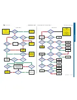
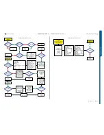
 Audio External Problems

Fault Trace SW

Audio and FM Radio

Audio Loop test

Audio Input: Mic1

Loop Mode: Analog

Audio Output:

Earphone

Apply Audio Loop

Blow into the 

PBA Mic

SL 5 Replace

 N2000

SL 4 Escalate

Yes

Replace

B3100

Yes

More than

100m Volt AC Pk-Pk

at MP 14 (L3103 BEARP)

 and MP 15 (L3104 BEARN)

when blowing in the PBA

Mic

No

2.2 Volt DC

at

 MP 27 (R3131)

No

More than

100mVolt AC Pk-Pk

at MP 28 (R3132) when

blowing in the

PBA Mic

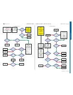
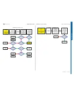
Fault Trace SW

Audio and FM Radio

Audio Loop test

Audio Input: Mic1

Loop Mode: Analog

Audio Output: Loudspeaker

Apply Audio Loop

Whistle as close as possible

in the PBA Mic

More than

100mVolt AC Pk-Pk at

MP 54 (X3102) and MP 53

(X3103) when whistle in

the PBA Mic

Yes

No

No

SL 5 Replace

 N2000

SL 4 Escalate

More than

100m Volt AC Pk-Pk at

 MP 17 (X3100) and MP 16

(X3101)

when blowing in the

PBA Mic

Yes

No

SL 5 Replace

V3101, V3102,

L3103 or L3104

SL 4 Escalate

1.9 Volt DC

at MP 54 (X3102) and

MP 53 (X3103)

Yes

No

Go to 

Audio External

Problems

No

Are any of

V3105, V3106

C3137 or C3123

short circuit

SL 4 Replace

V3105 or V3106

SL 5 Replace

C3137 or C3123

Replace

N3100

More than

100mVolt AC Pk-Pk

at MP 35 (C3137) and MP
36 (C3123) when whistle

in the PBA

Mic

No

Yes

1.9 Volt DC

at MP 56 (L3108) and

MP 55 (L3109)

No

Yes

Yes

SL 5 Replace

D2000

SL 4 Escalate

1.8 Volt DC

at MP 18 (R3137

AMPCTRL)

Yes

No

No

0 Volt DC at

MP 109

(V2420_Cathode)

Yes

Replace

N2400

SL 5 Replace

L3108 and L3109

SL 4 Escalate

Replace

V2405

No

Are any of

V3103 and V3104

Short circuit

SL 5 Replace

V3103 or V3104

SL 4 Escalate

Yes

Fault Trace SW

Logic

GPIO Manager

Access:

Set GPIO_03 to High

Application:

Set GPIO_01 to High

Access

GPIO_02 Read

1.8 Volt DC

at MP 21 (R2435)

SL 5 Replace

D2000

SL 4 Escalate

No

2.6 Volt DC

at MP 22

(V2405_ Pin 5)

Yes

0 Volt DC

at MP 23 (V2405_Pin

3) and Access: Result

GPIO_02=HIGH

Yes

Yes

No

SL 4 Replace

V2420

SL 5 Replace

R2440

START

Step1

If Mic problem go to step 2.

If Loudspeaker or Earphone problem

replace Speaker Box or Earphone and

retest the phone. If successful claim

Speaker Box or Earphone

If not then go to step 2.

Step 2:

Perform

System Connector Protection Test.

If the test is pass go to step 2

Step 3:

Load ITP SW into the phone.

Use TRS Fixture.

Connect VBATT and DCIO/SEPI

and continue with the

Audio Internal Problems TRS guide

No

Yes

Audio Internal problems

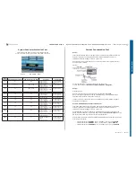
START

Step 1: 

Perform

System Connector Protection

Test

If the test is pass go to step 2

Step 2:

Load ITP SW into

the phone.

Use TRS Fixture

Connect: VBATT and DCIO/SEPI

Use Fault Trace SW and

continue with the Audio External

Problems TRS guide.

Fault trace SW

Audio and FM Radio

Audio Loop Test

Audio Input: AUX1

Loop Mode: Analog

Audio Output:

AUX Earphone

Apply Audio Loop

Replace

L2403 or L2404

Can you

 hear anything in

AUX earphone when

blowing into the

AUX Mic

No

More than

100mV AC Pk-Pk

at MP 33 (C3124 MICP_int)

and MP 30 (C3125 MICN_int)

when blowing in to the

AUX mic

Yes

More than

100mV AC Pk-Pk

At MP 104 (C2415 SPR)

and MP 103 (C2416 SPL) 

when blowing in to the 

AUX mic

Is

L2403 and L2404

Max 2 Ohm

No

Yes

Replace

System Connector

X2300

Yes

No

Disconnect

DCIO/SEPI cable

and Insert PHF set

Blow into the

AUX Mic

Is

MP 108

(X2300_Pin 9)
Connected to

MP 106 (L2402)

No

Yes

 Is

MP 107

(X2300_Pin 10)

Connected to

MP 105 (L2401)

No

Yes

No

Yes

Yes

L2401

Ok

Replace

L2401

L2402

Ok

Replace

L2402

No

No

Yes

 Audio Internal

Tested

Yes

No

More than

100mV AC Pk-Pk

at MP 32 (C3113) and

MP 29 (C3120) when

blowing in to the

AUX mic

Replace

N3101

Yes

SL 4 Replace

C3113 and C3120

SL 5 Replace

N2000

No

Replace

System Connector

X2300

Replace

N3101

2.2 Volt DC at

MP 99 (C3169)

Yes

SL 5 Replace

N2000

SL 4 Escalate

No

Replace

System Connector

X2300

Go to

Audio Internal

problems

Flash the phone

with

EMMA SUCR SW

Disconnect
VBATT and

DCIO/SEPI

Audio External  problems

SEMC Troubleshooting Manual

17

 (115)

Summary of Contents for C702

Page 1: ...C702 1221 7857 rev 1 Troubleshooting Manual APPENDIX COMPONENT OVERVIEW FUNCTIONAL OVERVIEW ABOUT ABOUT TROUBLESHOOTING MEASUREMENT POINTS C702 SEMC Troubleshooting Manual 1 115 ...

Page 2: ...roblems 20 System Connector Protection Test 21 Current Consumption Test 21 Current Consumption Test 22 Battery and Current Calibration Test 23 Backup Capacitor Test 23 Charging Test 24 ASIC Revision Test 24 Reference Measurement Points 25 Measurement Points Pictures 26 MEASUREMENT POINTS 39 Front Side 39 Back Side 40 N1200 Thor Module 41 N1210 Squid Module 42 Top Schematic 43 Imaging Top 44 Imagin...

Page 3: ...annel 1 VBATT and the dummy battery must be maximum 1m The cable must have a capacity for at least 16A Note It is very important to follow instrument settings instructions when performing the Battery Calibration Test Power Supply Channel 2 DCIO SEPI Agilent 6632B or similar Location CSPN Repair Instructions Level Mechanical Tool Catalogue Instrument Settings Voltage 5 0 Volt Limiter 2A Note It is ...

Page 4: ...cation CSPN Repair Instructions Level Mechanical Tool Catalogue See Picture 4 Picture 4 DSU 60 USB Cable Location CSPN Repair Instructions Level Mechanical Tool Catalogue Part number KRY 101 1413 RF Test Cable Flexible Location CSPN Repair Instructions Level Mechanical Tool Catalogue Part number RPM 119 885 See Picture 5 Picture 5 SEPI Interface Cable A1 Location CSPN Repair Instructions Level Mec...

Page 5: ...ect the CST 75 charger Red or White wire to the Plus Output and the Black wire to the Minus GND Output at Power Supply Channel 2 DCIO SEPI according to Picture 8 Picture 8 STEP 3 Cut of isolation material from inside of the charger plug according to Picture 9 Picture 9 STEP 4 Connect DCIO and SEPI Interface Cable A1 cables according to Picture 10 Picture 10 This is wrong setup see picture 11 Pictu...

Page 6: ...acturer PMK Germany Location http www elfa se en or other supplier Part number 46 310 40 Note This is ELFA part number STEP 2 Cut the Red lab plug according to Picture 16 Picture 16 STEP 3 Use any Hands free PHF Cable and cut according to Picture 17 Picture 17 Note Minimum Cable length 40 cm STEP 4 Use only wire connected to Pin2 and cut all rest wires according to Picture 18 Use digital multimete...

Page 7: ...M GSM UMTS is needed to perform Current Consumption Test see Picture 21 Location To buy a Test SIM GSM UMTS please contact your supplier of test equipment Picture 21 Sony Memory Stick M2 Any functional Memory Stick Micro M2 Card see Picture 22 Picture 22 Rohde Schwarz RF Shield Package Box Location CSPN Repair Instructions Level Mechanical Tool Catalogue Picture 23 SMK RF Probe Location CSPN Repai...

Page 8: ...System Connector Protection Test If the test is pass go to step 2 Step 2 Use Phone with Normal SW Use TRS Fixture Connect Display Keypad and VBATT Dowload ITP SW into the Phone by using EMMA SW No SL 5 Replace Z4203 SL 4 Escalate 5 Volt DC at MP 118 C2414 Yes No Yes Yes Max 2 Ohm between MP 113 X2300_Pin 2 and MP 115 Z4203_Pin 4 No SL 5 Replace R2484 SL 4 Escalate Yes No Power Up the Phone Connect...

Page 9: ...s Ok Current Consumption more than 50mA Step 1 Disconnect VBATT and DCIO SEPI Step 2 Connect Display and Keypad to the PBA Step 3 Connect Only VBATT Step 4 Activate EMMA SW Press the C key and connect USB Cable from PC Flash the Phone with ITP SW Yes ITP SW Flash Successful SL 5 Replace D2020 SL4 Escalate Yes Go to Flash Problems No No SL 5 Replace N2000 SL 4 Escalate No SL 5 Replace D2000 SL 4 Es...

Page 10: ...olt DC at MP 2 ST4205 and 0 Volt DC at MP 1 C4228 Yes No Yes Yes SL 5 Replace N2000 SL 4 Escalate Fault trace SW MMI Display pattern Init Screen Testing Activate RGB Color Pattern 2 6 Volt DC at MP 4 ST4201 and 1 8 Volt DC at MP 3 ST4202 No START Step 1 Use TRS Fixture Connect Display Keypad and VBATT Start the Phone If the Display is working properly on the TRS Fixture then replace Display If not...

Page 11: ...e PBA Use Fault trace SW and go to MMI Misc Deactivate Display Backlight Fault trace SW MMI Misc Activate Display Backlight Display Illumination problems START Step 1 Use TRS Fixture Connect Display Keypad and VBATT Step 2 Perform Keyboard Test in Service Tests Menu If All Keys are working properly on the TRS Fixture then replace Keypad If not then continue with the Key Problems TRS guide part 1 P...

Page 12: ...eplace V4205 SL 4 Escalate No Yes 0 2 Volt DC at MP 11 V4205_Pin 1 Yes SL 5 Replace N2000 SL 4 Escalate No Flash the Phone with EMMA SUCR SW 0 3 Volt DC at MP 60 TP2004 Replace X2402 Yes No Problem with Lower Keypad LED 0 8V 0 9V DC at MP 61 TP2003 Yes Yes SL 5 Replace V4205 SL 4 Escalate No 0 7V 0 8V DC at MP 12 V4205_Pin 4 Yes SL 5 Replace N2000 SL 4 Escalate No Problem with Camera Keypad LED 3 ...

Page 13: ...isc Init Screen Testing Activate VGA Camera Test 2 Logic GPIO Manager Application GPIO Read GPIO_02 and GPIO_09 Yes Is the Application Result GPIO GPIO_02 HIGH and GPIO_09 LOW Retest Main and VGA Camera Yes Is the problem with Main Camera Replace VGA Camera SL 5 Replace D2000 SL 4 Escalate No No Replace Main Camera Yes Main Camera Ok Claim Main Camera Yes Replace X4301 No No VGA Camera Ok Claim VG...

Page 14: ...ound No Yes SL 5 Replace C4206 C4207 L4202 SL 4 Escalate Scrap PBA START Step 1 Load ITP SW into the phone Step 2 Use TRS Fixture Connect VBATT and DCIO SEPI Use Fault Trace SW and go to MMI Misc Init Screen Testing Activate Vibrator Test NOTE If the Vibrator is working properly on the TRS Fixture then replace vibrator if not then continue with Vibrator Problems TRS guide Is L4204 Max 1 5 Ohm Yes ...

Page 15: ...ace System Connector X2300 Phone consuming more than 10mA Charger Current DCIO SEPI Yes Start Current Calibration C C SL 5 Replace R2201 SL 4 Escalate Replace V2202 R2201 0 3 Ohm No MP 46 C2241 DCIO_INT Higher than 3 8 Volt DC MP 121 R2201 CHSENSEP Higher than 3 8 Volt DC During C C MP 119 V2202_Pin 2 CHREG Lower than MP 46 C2241 During C C Yes No Yes No Phone Consuming DCIO SEPI Current During Cu...

Page 16: ...0 Kohm Between MP 96 X2403_Pin1 Red Probe and MP 90 X2403_Pin 7 Black Probe SL 5 Replace R2419 SL 4 Escalate No Yes 1 8 Volt DC at MP 47 C2406 No Replace X2403 Yes 1 8 Volt DC at MP 111 X2403_Pin 2 No Replace X2403 0 9V 1V DC at MP 93 V2407 No Yes SL 4 Replace X2403 SL 5 Replace V2408 SL 5 Replace N2000 SL 4 Escalate SL 5 Replace N2000 SL 4 Escalate 1 8 Volt DC at MP 92 V2404 SL 5 Replace N2000 SL...

Page 17: ...t MP 23 V2405_Pin 3 and Access Result GPIO_02 HIGH Yes Yes No SL 4 Replace V2420 SL 5 Replace R2440 START Step1 If Mic problem go to step 2 If Loudspeaker or Earphone problem replace Speaker Box or Earphone and retest the phone If successful claim Speaker Box or Earphone If not then go to step 2 Step 2 Perform System Connector Protection Test If the test is pass go to step 2 Step 3 Load ITP SW int...

Page 18: ...45 or C3146 Short circuit Replace V2425 No FM Radio Problems START Step 1 Flash the phone with EMMA SUCR SW and retest the phone If successful claim SW Flashing If not then go to Step 2 Step 2 Continue with the Bluetooth Problems TRS guide Fault trace SW TX and RX Bluetooth Channel 0 Set MaxPwr MOD 0 Use Spectrum Analyzer Instrument settings Frequency 2402 MHz Span 1MHz Amplitude 5dBm BW Auto Use ...

Page 19: ...tched GSM Radio Settings Select Band GSM 850 Channel 128 Power Level 5 No 1 4V 1 6V Pk Pk Pulses at MP 123 R1000 VAPC Replace N1200 No Fault Trace SW Switch GSM Mode Settings to TX Static Yes Use Spectrum Analyzer Instrument settings TX Freq 824 2 MHz Span 300 kHZ Amplitude 5 dBm BW 1 kHz Use RF Probe with 10 1 Divider Signal at MP 122 Z1001 20 dBm 5dBm SL 5 Replace N1002 SL 4 Escalate No Fault Tr...

Page 20: ...V 3 8V DC at MP 83 R2210 VBATI No SL 5 Replace R2210 SL 4 Escalate No 1 8Volt DC at MP 85 R2299 DCDC_EN 1 8V at MP 125 C417 WPA0_EN Squid Yes SL 5 Replace D2000 SL 4 Escalate No 1 2V 1 8V DC at MP 86 ST2217 WPAVCC Yes SL 4 Replace N2205 SL 5 Replace L2207 Yes 26MHz at MP 126 C511 WBCLK Squid No Replace N1200 Replace N1210 No Yes Go to SERP Calibration Go to SERP Calibration WCDMA Network Problems ...

Page 21: ... Current Consumption Test Step 1 Insert Local SIM Card and use the phone with the Normal SW SSW and dummy battery connected to Power Supply Channel 1 VBATT according to Picture 1 Instrument settings Voltage 3 8 Volt Limiter 3A Measure the current when Phone is off Check the current consumption at Power Supply Channel 1 VBATT Picture 1 Current consumption in off mode should be less than 1mA If more...

Page 22: ...t Band GSM 900 Channel 1 Power Level 5 GSM Radio Settings Select Band DCS 1800 Channel 512 Power Level 0 Max TX Power PCS 1900 MHz Fault Trace SW settings TX and RX GSM GSM Mode Settings TX Switched GSM Radio Settings Select Band PCS 1900 Channel 512 Power Level 0 Max TX Power WCDMA BAND I Fault Trace SW settings TX and RX WCDMA Radio Settings Select Band BAND I Fast Select Channels Ch LOW Modes M...

Page 23: ...ower Supply Channel 1 VBATT 3 8 Volt Limiter 2A Power Supply Channel 2 DCIO SEPI 5 0 Volt Limiter 2A Use dummy battery according to the Equipment List for this test Limits Table for the Current Calibration Test Measured Current Name Min Max Unit 100mA DCIO Current 50 150 mA 800mA DCIO Current 725 875 mA Backup Capacitor Test To perform this test use Phone with ITP SW Power Supply Channel 1 VBATT I...

Page 24: ...nt If the charging current is Not equal to the reference table go to Charging problems TRS Guide If the charging current is equal to the reference table then insert the normal battery and test the charging current to verify that the phone battery is working properly Measure the voltage at the battery to check the current level If the battery is receiving the right current then the phone and the ba...

Page 25: ...7V 26MHz FM Radio N1400 Use Fault Trace SW to activate and deactivate FM Radio MP MP 80 TP2200 MP 20 ST2207 MP 5 R2101 Power sup 3 80 Volt VBATI VDDE18 BT_CLK FM Radio Off 3 8V 1 8V 26MHz FM Radio On 3 8V 1 8V 26MHz Main and VGA Camera Use Fault Trace SW to activate and deactivate Main and VGA Camera Main and VGA Camera must be connected to the PBA MP MP 72 TP2204 MP 77 TP2210 MP 71 TP2207 MP 52 T...

Page 26: ...C702 1221 7857 rev 1 TROUBLESHOOTING Measurement Points Pictures TROUBLESHOOTING MP 6 R2120 MCLK MP 5 R2101 BT_CLK SEMC Troubleshooting Manual 26 115 ...

Page 27: ...C702 1221 7857 rev 1 TROUBLESHOOTING TROUBLESHOOTING Measurement Points Pictures MP 39 R2122 RTCCLK MP 38 V2400_Pin 3 SEMC Troubleshooting Manual 27 115 ...

Page 28: ...C702 1221 7857 rev 1 TROUBLESHOOTING TROUBLESHOOTING Measurement Points Pictures MP 42 C2106 32 kHz MP 41 C2103 32 kHz SEMC Troubleshooting Manual 28 115 ...

Page 29: ...C702 1221 7857 rev 1 TROUBLESHOOTING TROUBLESHOOTING Measurement Points Pictures MP 64 Z1400_Pin 7 MP 63 Z1400_Pin 5 SEMC Troubleshooting Manual 29 115 ...

Page 30: ...C702 1221 7857 rev 1 TROUBLESHOOTING TROUBLESHOOTING Measurement Points Pictures MP 76 ST4304 13 MHz MP 65 Z1400_Pin 1 SEMC Troubleshooting Manual 30 115 ...

Page 31: ...C702 1221 7857 rev 1 TROUBLESHOOTING TROUBLESHOOTING Measurement Points Pictures MP 97 SP2102 SYSCLK1 MP 82 C4206 SEMC Troubleshooting Manual 31 115 ...

Page 32: ...C702 1221 7857 rev 1 TROUBLESHOOTING TROUBLESHOOTING Measurement Points Pictures MP 122 Z1001 THOR MP 100 X1302 BT_ANT SEMC Troubleshooting Manual 32 115 ...

Page 33: ...C702 1221 7857 rev 1 TROUBLESHOOTING TROUBLESHOOTING Measurement Points Pictures MP 124 C1014 THOR MP 123 R1000 VAPC THOR SEMC Troubleshooting Manual 33 115 ...

Page 34: ...C702 1221 7857 rev 1 TROUBLESHOOTING TROUBLESHOOTING Measurement Points Pictures MP Z4200_Pin 1 and 5 MP 126 C511 WBCLK SQUID SEMC Troubleshooting Manual 34 115 ...

Page 35: ...C702 1221 7857 rev 1 TROUBLESHOOTING TROUBLESHOOTING Measurement Points Pictures MP Z4200_Pin 3 and 7 MP Z4200_Pin 2 and 6 SEMC Troubleshooting Manual 35 115 ...

Page 36: ...C702 1221 7857 rev 1 TROUBLESHOOTING TROUBLESHOOTING Measurement Points Pictures MP Z4201_Pin 1 and 5 MP Z4200_Pin 4 and 8 SEMC Troubleshooting Manual 36 115 ...

Page 37: ...C702 1221 7857 rev 1 TROUBLESHOOTING TROUBLESHOOTING Measurement Points Pictures MP Z4201_Pin 3 and 7 MP Z4201_Pin 2 and 6 SEMC Troubleshooting Manual 37 115 ...

Page 38: ...C702 1221 7857 rev 1 TROUBLESHOOTING TROUBLESHOOTING Measurement Points Pictures MP Z4201_Pin 4 and 8 SEMC Troubleshooting Manual 38 115 ...

Page 39: ...3209 SP3201 R2485 SP3204 SP3207 C2230 SP3208 R2211 ST4300 C2339 SP3205 C2417 C2313 C2338 R2220 SP5104 SP5103 SP5102 ST2208 ST2210 C3138 C2209 ST2209 ST2205 R3129 ST2213 C2405 V2400 C2406 R3128 ST2401 R2419 C2226 C2242 C2241 C2215 C3135 C3129 C2200 C2229 R3135 ST2302 C2225 C2205 C3130 R2435 N2400 SP2113 C2337 C2412 R2437 V2405 R3304 R2438 SP4300 C2335 C2322 C2430 C2314 C2330 SP2121 SP2132 C2336 C23...

Page 40: ...1 1 0 0 0 0 N N8 81 10 00 0 C C8 81 10 08 8 C C 8 8 1 1 0 0 1 1 C C 2 2 2 2 8 8 0 0 L L 8 8 1 1 0 0 0 0 R R8 81 10 06 6 C C 8 8 1 1 0 0 2 2 ST8100 TP4200 TP4201 X X 2 2 4 4 0 0 3 3 R R3 31 11 16 6 N N 3 3 1 1 0 0 0 0 R R2 24 45 50 0 TP2003 C C3 31 10 04 4 C C 3 3 1 1 0 0 6 6 R R3 31 11 15 5 R R2 24 45 51 1 C C2 24 44 43 3 C C2 24 44 41 1 R R2 24 45 52 2 C C3 31 10 05 5 R R2 24 45 53 3 C C2 24 44 4...

Page 41: ...0 0 1 Z L1006 B1100 3 1 0 1 C 2 0 0 1 L 4 0 0 1 L C1116 6 0 1 1 C 1 0 1 1 C 2 0 1 1 C 4 1 1 1 C 3 1 1 1 C 9 0 1 1 C 0 1 1 1 C 5 0 1 1 C 0 2 0 1 C 6 1 0 1 C 3 0 0 1 C 2 0 0 1 C C1117 C1015 C1014 4 0 0 1 C 5 0 0 1 C 8 1 1 1 C 1 0 0 1 C 9 1 1 1 C L1101 L1100 3 0 1 1 L 2 0 1 1 L 1 0 0 1 L 0 0 0 1 L 0 0 0 1 C 2 1 0 1 C N1001 Z1000 MP 124 MP 123 MP 122 N1200 Thor Module SEMC Troubleshooting Manual 41 11...

Page 42: ...0 N2001 N3001 C102 C103 C510 R504 R501 C509 C508 C416 C415 R503 R 5 0 2 R402 C420 C203 C506 C507 C204 C414 R203 R201 R202 R204 C511 C419 C417 C418 R405 Z301 R403 C201 C206 L207 L206 Z201 L205 C304 C301 C302 C303 S100 MP 126 MP 125 N1210 Squid Module SEMC Troubleshooting Manual 42 115 ...

Page 43: ..._EN VAUDIO26 CAMSYSCLK KB_LED KB_LED1 VBOOST VBATI VDDE18 VCAMIO VCAMAF VCAMSA I2CCLK1 I2CDAT1 KB_LED2 VCAM12 Imaging Pages I1 I4 X1430 1 X1431 1 X1201 1 X1202 1 X1203 1 E1000 1 SHIELDCAN_NING_BASE_BB 1202 0856 Will be connected to GND in PCB Clamp GND E1001 1 SHIELDCAN_NING_GPS 1202 0850 Will be connected to GND in PCB Clamp GND E1002 1 SHIELDCAN_NING_MP202 1202 0851 Will be connected to GND in P...

Page 44: ...VDDE18 VAUDIO26 FLASH_TORCH VDIG I05_Sensor FLASHLED_CA STEPUP50 I2CDAT1 VCAMIO VCAM12 VDDE18 VCAMAF VCAMSA CAMSYSCLK I2CCLK1 I03_Camera VCAM_SA_EN CAM_STORB FLASH_TORCH VDDE18 VBATI I2CCLK1 I2CDAT1 I04_LMU STEPUP50 FLASHLED_CA CAM_STORB VBATI VDDE18 VCAMSA VCAMIO VCAMAF VBATI VDDE18 VCAMAF VDDE18 VCAMSA VCAMIO I2CCLK1 CAMSYSCLK I2CDAT1 KB_LED1 KB_LED2 VBOOST KB_LED VBATI VDDE18 VAUDIO26 VAUDIO26 ...

Page 45: ... 1A C E B R4222 0ohms 2 2uF C4200 25V 1uF C4208 25V 1uF C4203 1000 7420 NM B4200 2 1 VIBR_B3ASL2723 VIBRATOR A B KB_LED2 10Kohms R4207 1200 0320 BC847CDXV6T1G 6 1 2 1A V4206 C E B 1000 0426 MEA2010LC220T002 1 2 3 4 5 6 7 8 9 10 Z4202 GND_2 GND_1 O4 2 O3 2 O2 2 I4 1 I3 1 I2 1 I1 1 O1 2 EMI FILTER 1000 0426 Z4201 9 0 1 8 7 6 5 4 3 2 1 MEA2010LC220T002 GND_2 GND_1 O4 2 O3 2 O2 2 I4 1 I3 1 I2 1 I1 1 O...

Page 46: ...a PoP bottom IMAGING CI_RESn CI_D7 CI_D6 CI_D5 CI_D4 CI_D3 CI_D2 CI_D1 CI_D0 CI_VSYNC CI_HSYNC CI_PCLK D2000 V15 ANJA Bottom 1200 0186 APPLICATION GPIO_02 VCAM_SA_EN D2000 R22 ANJA Bottom 1200 0186 APPLICATION GPIO_09 D2000 R23 ANJA Bottom 1200 0186 APPLICATION GPIO_08 R4311 100Kohms 0ohms NM R4313 SP4301 1 GND 2 D0 3 D1 4 D2 5 D3 6 D4 7 D5 8 D6 9 D7 12 DCK 13 SCL 14 SDA 15 GND 16 GND_AF 17 VDD_AF...

Page 47: ...5 C4 D4 E1 C1 A1 D3 B1 E4 F4 C5 F1 D1 N8100 LMU 1 1200 2296 LP55271 VREF GNDA GND_LED GND_FLASH GND_SW2 GND_SW1 IFLASH FLASH LED4 LED3 LED2 LED1 FB SW1 ASE1 GND ASE2 VDDIO FLASH_SYNCK SDA SCL T1 RT VDDA VDD2 VDD1 NRST SW2 GNDC T2 CUS01 V8100 1002 0000 330pF C8575 FLASHLED_CA D2000 P24 ANJA Bottom 1200 0186 APPLICATION GPIO_06 D2000 APPLICATION GPIO_07 N25 ANJA Bottom 1200 0186 APPLICATION GPIO_07 ...

Page 48: ...4 D2000 APPLICATION GPIO_10 1200 0186 APPLICATION GPIO_10 R4224 270Kohms R4225 470Kohms R4231 10Kohms VDIG NM V2201 ESD5B5 0ST1G 1201 0304 1 A 2 A 0 1uF C8122 A3 VOUT_MR A4 GND A5 VIN_FLASH B1 VIN_FLASH B2 VIN_FLASH B3 TORCH_FLASH B4 SINK_FLASH B5 SINK_FLASH Z1 Z2 Z3 Z4 STEPUP50 FLASH_TORCH A1 X4201 VIN_MR 1202 0859 A2 GND C8121 39pF ST4206 2 1 VDIG VDIG FLASHLED_CA STEPUP50 FLASH_TORCH MP 78 SEMC...

Page 49: ...T27 ANT MCLK TESTOUT DCDC_EN TX_ADSTR WPAVCC AGPSANT FM_AGPSRESn BT_CLKREQ VBT27 VDDE18 VDIG RTCCLK BTRESn BT_CLK Bluetooth Page 3 Page 3 Bluetooth FM_AGPSRESn BT_CLK TX_ADSTR RTCCLK AGPSANT VDDE18 R04_AGPS VAGPS20 VAGPS28 VAGPS20 VAGPS28 GSM UMTS ANTSW0 ANTSW1 ANTSW2 ANTSW3 MCLKREQ AMP_LSB_FREQ_LSB RADCLK RADDAT RADSTR VBATI VDDE18 VccA VCC_WPA IDATA_FREQ_MSB QDATA_AMP_MSB WDETON TXIA TXIB TXQA T...

Page 50: ... GND13 GND14 GND15 GND16 GND17 GND18 GND19 GND20 GND21 GND22 GND23 GND24 GND25 GND26 GND27 GND28 GND29 GND30 47ohms R1200 47ohms R1201 WPA0_EN TXIA TXIB TXQA TXQB RXIA RXIB RXQA RXQB WPAVCC 1000 8181 X1200 4 3 6 5 2 1 CRS5001 R_TERM C_TERM GND GND GND GND WTXPOWDET 1 2pF NM C1203 56pF C1211 56pF C1212 C1204 0 5pF NM 0ohms R1207 1200 0050 U300_WCDMA_SQUID SH1 A3 A2 A4 A5 A6 B6 C6 B1 C1 D1 E1 F1 H3 ...

Page 51: ...T_HVA2 BT_VIO_A BT_VIO_B BT_VIO_C BT_VIO_D BT_VIO_E BT_VDD_CLD BT_VSS_ANA BT_VSS_ANA BT_VSS_ANA BT_VSS_ANA BT_VSS_ANA BT_VSS_ANA BT_VSS_ANA BT_VSS_ANA BT_VSS_ANA BT_VSS_ANA BT_VSS_ANA BT_VSS_ANA BT_VSS_DIG BT_VSS_DIG BT_VSS_DIG BT_VSS_DIG BT_VSS_DIG BT_VSS_RF BT_VSS_RF BT_VSS_RF BTPOWER GND BT_VSS_RF 1200 6182 STLC2592 G6 E7 F9 J7 J8 L7 M7 N6 G9 L3 M3 K4 K3 J3 K5 M5 M4 N4 F6 J4 J1 K1 B2 C3 M8 C1 C...

Page 52: ...6 E6 F1 F3 C7 E3 D3 G2 E2 E1 F2 D4 C6 5 C 5 B D6 N1430 PMB2525 1200 0700 RTCCLK POWERON RX_HOLD nRESET SYNC CNTIN CLK nINTR OMS0 OMS1 OMS2 HIF0 HIF1 HIF2 HIF3 HIF4 HIF5 MIX_IN_PLUS MIX_IN_MINUS LNA_OUT LNA_IN EXT_LNA TDI TMS TCK nTRST TDO PMB2525_Hammerhead _Power_distribution SYSCON ConfigHostIFI2C SPI UART HostIF RF JTAG E7 D1 C1 G1 G3 B7 C2 A7 B6 B4 A6 A5 G5 F4 F7 D7 D5 D2 B1 E4 G4 E5 N1430 1A ...

Page 53: ...N AUXinR I2CCLK1 TX_ADSTR I2CDAT1 VAD VBACKUP VDDE18 SPL SPR VMC18 TESTOUT VBUS ONSWAn VBOOST KB_LED KB_LED1 MICP AUXinL FM_ANTENNA DCON Pages 11 16 Connectivity VCAM_SA_EN VAGPS28 VAGPS20 Pages 6 10 Power VCAM12 VCAM_SA_EN VAGPS28 VAGPS20 AGPS_LDO_EN DCDC_EN VBUS DCIO WPAVCC VBT27 VDDE18 VCAMAF VBEAR26 VMC18 VCAMIO VBACKUP VDIG VBATI VCAMSA VAUDIO26 VccA VCC_WPA VDDE18_ANJA VDD_LP Power Pages 6 1...

Page 54: ...Q RTCCLK FM_AGPSRESn Memories Page 4 VDDE18_ANJA MEMRESn Memories Page 4 VDDE18_ANJA VDD_LP SYSCLK2 DCON Page 3 AGPS_LDO_EN DCON SYSCLK2 VDDE18 BT_CLKREQ SERVICEn ONSWAn MCLK FM_AGPSRESn RTCCLK BT_CLK MCLKREQ MEMRESn BTRESn CAMSYSCLK VDD_LP Clocks Resets Page 3 AGPS_LDO_EN VDDE18 VDDE18 BT_CLKREQ MCLK SERVICEn ONSWAn BT_CLK CAMSYSCLK RTCCLK MCLKREQ BTRESn MEMRESn VDDE18_ANJA VDD_LP VDD_LP DCON FM_...

Page 55: ...AD19 AB17 AD18 AE18 AC23 T13 AD22 AE22 AC16 AB16 AB23 AD17 AB20 D2000 1A 1200 0186 POWER CONTROL RESETS INTERRUPTS CLOCKS Anja PoP bottom SYSTEMLEVEL DCON APPSLEEP ACCSLEEP RESOUT2n RESOUT1n RESOUT0n SYSCLK2 SYSCLK1 SYSCLK0 MCLKREQ SERVICEn PWRRSTn MSAPPIRQn MSACCIRQn SYSCLK0REQn RTCCLKIN MCLK SP2104 SP2106 SP2107 SP2108 VDD_LP NM B2100 12 5 7 1 11 10 9 8 4 3 2 6 SG 3030LC 1200 3231 NC_10 NC_9 NC_...

Page 56: ...P_SDBS1 AP_A14 AP_SDBS01 AP_A13 AP_SDBS0 AP_A12 AP_A11 AP_A10 AP_A09 AP_A08 AP_A07 AP_A06 AP_A05 AP_A04 AP_A03 AP_A02 AP_A01 AP_WAITn AP_NF_READY AP_D15 AP_D14 AP_D13 AP_D12 AP_D11 AP_D10 AP_D09 AP_D08 AP_D07 AP_D06 AP_D05 AP_D04 AP_D03 AP_D02 AP_D01 AP_D00 1200 0186 ANJA Bottom D2000 D2 E2 J10 F2 F3 G2 G3 H3 J3 J2 K2 K3 L2 L3 M3 E5 B5 E3 E4 F4 F5 G4 G5 H4 H5 J4 J5 K4 K5 L4 L5 M4 M5 D3 C6 D6 C7 D4...

Page 57: ... TOP_SH_D08 TOP_SH_D09 TOP_SH_D10 TOP_SH_D11 TOP_SH_D12 TOP_SH_D13 TOP_SH_D14 TOP_SH_D15 TOP_SH_D00 TOP_SH_D01 TOP_SH_D02 TOP_SH_D03 TOP_SH_D04 TOP_SH_D05 TOP_SH_D06 TOP_SH_D07 TOP_SH_D08 TOP_SH_D09 TOP_SH_D10 TOP_SH_D11 TOP_SH_D12 TOP_SH_D13 TOP_SH_D14 TOP_SH_D15 TOP_AP_D14 TOP_AP_D15 TOP_AP_D13 TOP_AP_D00 TOP_AP_D01 TOP_AP_D02 TOP_AP_D03 TOP_AP_D04 TOP_AP_D05 TOP_AP_D06 TOP_AP_D07 TOP_AP_D08 TOP...

Page 58: ...18_ANJA VDD_LP VCAM_SA_EN Regulators Charging Page 7 AGPS_LDO_EN VDD_LP VCC_WPA VBT27 VBEAR26 VCORE18 VMC18 DCIO VBACKUP VBATI VDDE18 VCORE12 VANA25 VBUS VDIG VAUDIO26 VccA DCDC_EN WPAVCC VAGPS20 VAGPS28 Page 7 Regulators Charging AGPS_LDO_EN VAGPS20 VAGPS28 Page 8 Power Camera VCAM12 VCAMIO VBATI VCAMSA VCAMAF VCAM_SA_EN Page 8 Power Camera VCAM12 VBUS DCIO VBATI VBATI VBATI VCORE12 VCORE12 VAUDI...

Page 59: ...0uF 6 3V C2231 22pF NM C2237 22pF C2232 100nF C2234 100nF C2236 100nF L2207 3 3uH R2299 100Kohms C2235 4 7uF N2205 C1 C3 A2 C2 B1 A1 B3 A3 1A LM3208TLX 1200 0107 VCON EN PVIN VDD PGND SGND SW FB DCDC_COM DCDC_IO C2208 1uF VBT27 6 7 2 1 V2202 1A FDMA1027P 1200 0145 D D G S 3 8 5 4 V2202 1A FDMA1027P 1200 0145 D D S G C2238 1uF C2239 10uF R2222 NM 0ohms VCORE18 WPAVCC N2202 5 2 3 1 4 6 1A R1161D181B...

Page 60: ...GND C2293 NM 33pF 100Kohms R2211 100Kohms R2212 GND 1200 0186 ANJA Bottom T18 D2000 APPLICATION GPIO_03 APPLICATION GPIO_03 1200 0186 ANJA Bottom R25 D2000 APPLICATION GPIO_04 1200 0186 ANJA Bottom R24 D2000 APPLICATION GPIO_05 VCAM_SA_EN VCAM12 TP2207 1200 1852 N2212 1 3 TPS79913YZU A1 A3 C1 C3 B2 LDO REGULATOR EN IN OUT GND NR TP2204 C2294 10uF 0 01uF C2295 2 2uF C2299 ST2200 1 2 ST2201 1 2 ST22...

Page 61: ...4 AD3 AD2 AA2 W25 T2 L25 H2 D24 C25 C2 B25 B24 B17 B9 B6 B4 B3 B2 D2000 I2CRESETSUPPLY VDDCORE logic Anja PoP bottom POWER VDD1V2 VDD_1 VDD_1 VDDCO_1v2 VDDCO_1v2 VDDCO_1v2 VDDCO_1v2 VDDCO_1v2 VDDCO_1v2 VDDCO_1v2 VDDCO_1v2 VDDCO_1v2 VDDCO_1v2 VDDCO_1v2 VDDCO_1v2 VDDCO_1v2 VDDCO_1v2 VDDCO_1v2 VDDCO_1v2 VDDCO_1v2 VDDCO_1v2 VDDCO_1v2 VDDCO_1v2 VDDCO_1v2 VDDCO_1v2 VDDCO_1v2 100nF C2319 100nF C2322 100n...

Page 62: ...5 K14 K13 K12 K11 K10 J17 J16 1A ANJA Bottom 1200 0186 VDD_MEM VDD_MEM VDD_MEM VDD_MEM VDD_MEM VDD_MEM VDD_MEM VDD_MEM VDD_MEM VDD_MEM VDD_MEM VDD_MEM VDD_MEM VDD_MEM VDD_MEM VDD_MEM VDD_MEM VDD_MEM GND_MEM GND_MEM GND_MEM GND_MEM GND_MEM GND_MEM GND_MEM GND_MEM GND_MEM GND_MEM GND_MEM GND_MEM GND_MEM GND_MEM GND_MEM GND_MEM GND_MEM GND_MEM GND_MEM GND_MEM Anja PoP bottom POWER VDD MEMORIES C2345 ...

Page 63: ... Page 15 KB_LED2 VBOOST ONSWAn KB_LED KB_LED1 VDDE18 Page 15 Keypad KB_LED2 DCON Connectivity Page 14 SPL SPR VBATI VBUS SERVICEn FM_ANTENNA MICP AUXinL DCIO AID_AD MICN AUXinR VAUDIO26 VDDE18 SYSCLK2 DCON Page 14 Connectivity ADC DAC Page 12 TX_ADSTR I2CDAT1 I2CCLK1 VDDE18 VAD VBACKUP TESTOUT VAUDIO26 AID_AD ADC DAC Page 12 SYSCLK2 VDDE18 VDDE18 VBACKUP VDDE18 VMC18 VAD I2CDAT1 I2CCLK1 TESTOUT TX...

Page 64: ...3 GPA5 GPA6 GPA7 GPA12 TXON 1A N2000 C13 B13 AB3100 1000 8142 SDA SCL I2C IF Ericsson AB 3100 OP AND SERVICES TX_ADSTR C2400 100nF VAUDIO26 1A D2000 AB24 AA23 ANJA Bottom 1200 0186 APPLICATION I2C APP 1 Anja PoP bottom CONNECTIVITY I2CSCL2 I2CSDA2 1A D2000 AD23 AC24 ANJA Bottom 1200 0186 SHARED I2C IF ACC APP 0 Anja PoP bottom CONNECTIVITY I2CSCL I2CSDA R2421 4 7Kohms NM C2431 22pF R2442 4 7Kohms ...

Page 65: ...PoP bottom CONNECTIVITY SRSTn SCLK SDAT APPLICATION GPIO_12 T22 D2000 APPLICATION GPIO_12 VBATI 33pF C2428 NM 1 2 ST2400 1 2 ST2401 100nF C2429 SP2407 V2403 NM 1 2 DF2S6 8FS 1000 0282 A C V2404 DF2S6 8FS 2 1 1000 0282 A C V2407 DF2S6 8FS 2 1 1000 0282 A C V2408 DF2S6 8FS 2 1 1000 0282 A C GND GND GND GND 470Kohms R2406 33pF C2440 NM 33pF C2441 NM 33pF C2442 NM 33pF C2443 NM 33pF C2444 NM 33pF C244...

Page 66: ...00Kohms M9 ACCESS GPIO_01 P9 D2000 ACCESS GPIO_04 L9 ACCESS GPIO_00 R5 ACCESS GPIO_05 Y4 D2000 ACCESS GPIO_18 T4 ACCESS GPIO_06 T5 ACCESS GPIO_07 U5 ACCESS GPIO_08 1200 0186 ANJA Bottom U4 ACCESS GPIO_09 1200 0186 ANJA Bottom P17 D2000 APPLICATION GPIO_01 1200 0186 ANJA Bottom V5 D2000 ACCESS GPIO_16 1200 0186 ANJA Bottom R9 D2000 ACCESS GPIO_03 1200 0186 ANJA Bottom T3 D2000 ACCESS GPIO_02 100Koh...

Page 67: ...pF NM C2469 33pF NM C2468 33pF NM C2467 33pF NM C2465 33pF NM C2464 33pF NM C2463 33pF NM C2462 33pF NM C2461 33pF NM C2460 33pF NM C2459 33pF Chassi Z1 Chassi Z2 Chassi Z3 Chassi Z4 TP2003 TP2004 R2445 15Kohms R2446 15Kohms R2447 15Kohms R2448 15Kohms R2449 15Kohms R2444 15Kohms VDDE18 KB_LED2 TP2005 33pF C2458 NM GND ONSWAn 33pF NM C2426 V2402 LEADFREE 1000 0087 V2512 UESD3 3DT5G 3 1 2 1000 0399...

Page 68: ...6 RTCCLK Audio Digital Page 3 Page 3 Audio Digital Audio Analog Page 2 VBEAR26 VAUDIO26 VAD SPR SPL FML FMR MICP AUXinL MICN AUXinR VBATI Audio Analog Page 2 FM Radio FML FMR I2CCLK1 I2CDAT1 FM_ANTENNA RTCCLK VBATI VDDE18 FM_AGPSRESn Page 4 FM Radio VBATI VDDE18 VAUDIO26 VBEAR26 I2CDAT1 I2CCLK1 FM_ANTENNA MICN AUXinR MICP AUXinL VAD SPL SPR VBATI VDDE18 VBATI VAUDIO26 VBEAR26 FMR FML RTCCLK FM_AGP...

Page 69: ...0nF C3132 100nF C3133 100nF C3135 0ohms R3115 0ohms R3116 470nF C3145 470nF C3146 10uF C3112 220uF C3149 220uF C3150 2 2Kohms R3128 2 2Kohms R3129 0 1uH L3108 0 1uH L3109 33pF C3152 33pF C3151 470nF C3113 470nF C3120 24Kohms R3134 3 3nF C3155 V3101 1 2 DF2S6 8FS 1000 0282 A C V3102 DF2S6 8FS 2 1 1000 0282 A C GND GND V3103 DF2S6 8FS 2 1 1000 0282 A C V3104 DF2S6 8FS 2 1 1000 0282 A C GND GND C3160...

Page 70: ...C IF A 2 m o t t o B A J N A U23 T23 V24 U22 V23 W24 W23 U25 D2000 1200 0186 APP I2S PCM 1 APP I2S PCM 0 Anja PoP bottom AUDIO I2S1DLD PCM1DLD I2S1WS PCM1SYN I2S1CLK PCM1CLK I2S0DLD PCM0DLD I2S0WS PCM0SYN I2S0CLK PCM0CLK I2S1ULD PCM1ULD I2S0ULD PCM0ULD SP3201 SP3202 SP3204 SP3205 SP3206 SP3207 SP3208 SP3209 App_I2S1_CLK App_I2S1_WS App_I2S0_WS App_I2S0_CLK App_I2S0_DATA_A App_I2S1_DATA_A App_I2S0_...

Page 71: ... N1400 L6 L5 L4 F8 F7 D4 D6 B3 A4 D9 D8 E9 D7 C9 C5 5 B 8 C A5 A6 A7 D5 C7 C6 C4 B7 B6 B4 A3 B8 STLC2592 1200 6182 FM_PWR_GND FM_RADIO_IO FM_GND FM_GND FM_GND FM_GND FM_GND FM_GND FM_GND FM_GND FM_VIO FM_VD FM_VA NC NC NC NC NC NC FM_LOUT FM_ROUT FM_GPIO3 FM_GPIO2 FM_GPIO1 FM_RTCCLK FM_SDA FM_SCL FM_SENB FM_RST FM_RFGND FM_FMIP BLUETOOTH FM_FM L3300 0 27uH C3303 100pF 12pF C2227 ST3300 2 1 ST3301 ...

Page 72: ... PLL_416_FILTVDD PLL_416_VCONT PLL_26_FILTVDD PLL_26_VCONT 5 C 9 N D17 E23 G25 N23 V22 AB2 AC25 AE3 AE4 AE16 AE23 D2000 1A ANJA Bottom 1200 0186 UNUSED Anja PoP bottom NOTUSED NetUnused NetUnused NetUnused NetUnused NetUnused NetUnused NetUnused NetUnused NetUnused NetUnused NetUnused NetUnused EFUSE_HV4 SP5108 SP5109 SP5110 SP5111 SP5112 SP5113 SP5114 SP5115 SP5116 SP5117 SP5118 SP5119 SP5120 D20...

Page 73: ... X1 E8 X1 F1 X1 F2 X1 F7 X1 F8 X1 H1 X1 H2 X1 H7 X1 H8 X1 J1 X1 J2 X1 J3 X1 J4 X1 J5 X1 J6 X1 J7 X1 J8 X1 K1 X1 K2 X1 K3 X1 K4 X1 K5 X1 K6 X1 K7 X1 K8 X1 SH1 EDGERX WBCLK TESTOUT QDATA_AMP_MSB IDATA_FREQ_MSB DCLK_DATSTR MCLK AMP_LSB_FREQ_LSB RADCLK RADDAT RADSTR1 MCLKREQ GSMRX1900_1 GSMRX1900_2 GSMRX1800_1 GSMRX1800_2 GSMRX900_1 GSMRX900_2 GSMRX850_1 GSMRX850_2 PAM_MOD WCDMA850 WCDMA1900 WCDMA2100...

Page 74: ...KY77329 DCS_PCS_Out DCS_PCS_IN TX_EN BS GSM_IN GND3 GSM_OUT QuadbandPA GND4 GND5 GND6 GND2 GND1 GND_PAD VAPC VBATT NC2 NC1 R1000 0ohms C1020 NM 1 5pF C1012 NM 5 6pF C1013 NM 2 7pF C1014 NM 1 2pF C1017 22pF C1016 22pF C1003 22pF C1002 22pF C1000 22pF 1200 0169 1 4 5 6 16 17 18 19 11 12 13 9 14 15 21 22 20 7 24 23 10 8 3 2 Z1000 E DGM099M04 GND GND GND GND GND PCN PCS TX PCS RX PCS RX PCN RX PCN RX ...

Page 75: ...dA GndA GndA GndA DataStr DataC DataB DataA VccA Rx800n Rx800p Rx900n Rx900p Rx1800n Rx1800p Rx1900n Rx1900p RX Ericsson L1102 15nH L1103 18nH C1116 22pF C1117 10nF R1100 0ohms 1000 8134 P1T N1001 14 13 11 18 9 6 10 16 17 12 15 7 8 RF3000 CLASS SYNTH Ericsson Data Str MClkReq XOp XOn Clk VccD MClk WBClk TestOut GndA GndA GndD 1200 0097 B1100 3 1 4 2 KXS 23 26000KFA ZAOR I O I O COVER COVER C1118 2...

Page 76: ...N WPA0_EN WDETON RADDAT RADCLK RADSTR Vcc_PA VRAD_2V75 Vcc_PA WPAVcc VDIG_1V8 VBAT VRAD_2V75 WCDMA_ANT RXIA RXIB RXQA RXQB TXIA TXIB TXQA TXQB RADSTR RADCLK RADDAT WDETON WBCLK UMTS WTXPOWDET WPA0_EN WPA1_EN A1 A2 A3 A4 A5 A6 B1 B6 C1 C6 D1 D6 E6 F1 F6 H1 H2 H3 H4 H5 H6 SH1 E1 GND 1200 0085 SHIELDCAN_SQUID S100 1 Will be connected to GND in PCB Clamp GND GND 1200 0064 Page 1 6 Squid RF Module Radi...

Page 77: ...AT WDETON WPSENSE WPABIAS WPAVcc WTXPOWDET NM C506 10pF NM C507 10nF WBCLK N3001 4 6 5 2 7 1 3 LMV221 1200 0071 HEATSLUG GND OUT EN REF RF_IN VDD POWER DETECTOR C509 10pF C508 100nF N3000 11 22 21 15 39 38 23 14 12 13 RF3100 1000 8143 RF3100 PAO_1 PAO_2 TST GND_DIG REFIN CLK EN VGACTL DATA VDD CONTROL R504 1Kohms C510 33nF R502 220ohms C511 3 9pF R503 56ohms R501 56ohms 1200 0064 Page 2 6 Squid RF...

Page 78: ... Made for Document Nr Revision WCDMA_ANT_1 WCDMA_RX WCDMA_TX 1200 0074 1950 2140MHz DGLN38N01 Z101 2 4 5 7 8 9 1 3 6 LOWLOSS_Duplex ANT X T X R GND GND GND GND GND GND WCDMA_ANT GND 1 2pF C103 NM 22pF C102 1200 0064 Page 3 6 Squid RF Module Radio Duplex SEMC Troubleshooting Manual 78 115 ...

Page 79: ...QA RXQB WCDMA_ANT VRAD_2V75 RXIB RXQA RXQB RXIA WCDMA_RX Rx_UMTS TX_IB TX_QA Synt_UMTS TX_IA TX_QB WTXMOD WBCLK WDETON RADDAT RADCLK RADSTR VRAD_2V75 WTXPOWDET WPA0_EN WPA1_EN VBAT WCDMA_ANT Duplex WCDMA_RX WCDMA_TX RF_CONT_UMTS VRAD_2V75 VDIG_1V8 RADSTR RADCLK RADDAT WBCLK WDETON WPSENSE WPABIAS WPAVcc WTXPOWDET Vcc_PA WPA1_EN WPSENSE VBAT PA_UMTS WCDMA_TX WPABIAS WTXMOD WPA0_EN VRAD_2V75 1200 00...

Page 80: ... 8143 RF3100 36 N3000 31 24 20 19 18 17 32 33 35 29 27 30 26 25 34 37 28 GNDRX GNDRX GNDRX VCCLORX VCCRX MIX2_B MIX2_A LINA2_O LINA2_I MIX1_B MIX1_A LNA1_O LNA1_I GNDLNAEM RXIA RXQB RXQA RXIB RX RF3100 200ohms R201 200ohms R202 200ohms R203 200ohms R204 0 56pF C206 3 9nH L206 3 9nH L207 5 6pF C201 1 8nH L205 Z201 2 5 3 4 1 1001 1897 RF LOW LOSS SAW RFin GND GND RFout RFout 1200 0064 Page 5 6 Squid...

Page 81: ...10pF NM C303 10nF TX_IA TX_QB WTXMOD VRAD_2V75 TX_QA TX_IB 1 4 5 3 2 Z301 SAFEB1G95KA0F00 1200 0076 GND OUT IN GND GND 5 N3000 40 6 2 4 10 9 8 7 1 3 16 RF3100 1000 8143 RF3100 TXIA TXIB TXQA TXQB VCCLOTX VCCTX GNDTX GNDTX1 GNDTX2 GNDTXEM TX_2 TX_1 TX NM C304 1pF C301 NM 1pF 1200 0064 Page 6 6 Squid RF Module Radio Synthesizer UMTS SEMC Troubleshooting Manual 81 115 ...

Page 82: ...02 6 4 3 1 2 5 GND GND GND GND OUT IN ISOLATOR 10pF C418 0ohms R405 NM 0ohms NM R403 1200 0072 LDC181G9519B 327 K401 2 5 4 6 1 3 COUPL_OUT GND IN CLASS Power Coupler OUT TERM GND 10pF C417 22pF C419 10nF C413 1nF C414 1nF C415 10nF C420 1200 0073 1950MHz SKY77174 2 8 4 5 3 10 1 11 6 7 9 N2001 SKY771nn Module RFIN VCC1 VCC2 VBIAS VCONT ENABLE RFOUT GND GND GND GND_SLUG 22pF C416 1200 0064 Page 7 6 ...

Page 83: ...6 C2305 1000 0048 B6 C2307 1000 0048 C5 C2308 1000 0048 C6 C2311 1000 0048 B6 C2313 1000 0048 B5 C2314 1000 0048 C6 C2315 1000 0048 B5 C2316 1000 0048 B5 C2317 1000 0048 C5 C2318 1000 0048 B5 C2319 1000 0048 C5 C2322 1000 0048 C6 C2324 1000 0048 B6 C2326 1000 0048 B5 C2327 1000 0048 B5 C2328 1000 0048 B5 C2329 1000 0048 B5 C2330 1000 0048 B6 C2331 1000 0048 B5 C2332 1000 0048 B5 C2333 1000 0048 C6...

Page 84: ... 7 R R2 24 48 88 8 C C 2 2 4 4 3 3 4 4 R R2 24 48 81 1 C C 2 2 4 4 3 3 5 5 C C 2 2 4 4 1 1 6 6 R R2 24 48 87 7 V V2 24 42 20 0 V2411 R R 2 2 4 4 6 6 5 5 C C 2 2 4 4 1 1 3 3 R R 2 2 4 4 2 2 6 6 C C2 24 42 24 4 V V2 24 42 21 1 C C2 24 42 23 3 R R 2 2 4 4 6 6 6 6 C C2 22 20 01 1 V V2 22 20 02 2 L L3 31 10 00 0 L L3 31 10 01 1 V V 3 3 1 1 0 0 4 4 C C 3 3 1 1 6 6 2 2 X X 1 1 3 3 0 0 2 2 X X 1 1 3 3 0 0...

Page 85: ...net Access NetFront Web browser RSS feeds Communication Polyphonic ring tones Speakerphone Vibrating alert Video calling Messaging Email Instant messaging Picture messaging MMS Predictive text input Sound recorder Text messaging SMS Design Navigation key Picture wallpaper Wallpaper animation Entertainment 3D games FM radio Java Media Video streaming Video viewing Organizer Alarm clock Calculator C...

Page 86: ...LED driving Battery charging and communication circuitry Battery fuel gauging circuitry Analog to Digital Converter ADC SIM interface Six programmable LED drivers Accurate band gap reference Vibrator driver Real Time Clock RTC Eight byte One Time Programmable OTP memory Pulse Code Modulation PCM voice coder decoder PCM audio coder decoder Microphone interface Stereo line input Earphone driver Earp...

Page 87: ...ce with the particular period and duty cycle When the charging is on it is set to the current and voltage selected by I2C A low resistive path from VBAT to DCIO can be formed when DCIO is not detected When this setting is done in the appropriate registers a lowering of CHREG to 0 V turns on the external pass device The pass device is automatically turned off when an external source is detected on ...

Page 88: ...been powered down Block Diagram of the SIM Interface CODEC Overview The CODEC is encoding analog audio signals and analog voice signals into digital signals using ADCs This is done in the coder section of the CODEC also named the TX path transfer section The CODEC is also decoding digital audio signals and digital voice signals into analog signals using DACs This is done in the decoder section of ...

Page 89: ...sponsible for distributing clocks and resets to all parts of the Access subsystem This block is under SW control The Access subsystem is connected to the Shared EMIF an interface for communication with an external SDRAM The interface has 39 signals including one chip select and supports memory sizes up to 512 Mbit The Shared EMIF is shared between the Access subsystem and the Application subsystem...

Page 90: ...MA air interface mode the digital baseband controller controls the radio system through a 3 wire serial bus The digital baseband controller D2000 Anja also manages PA band control and the antenna switch mechanism in the front end module The 26 MHz VCXO clock residing in the GSM GPRS EDGE transceiver is turned on only when required The digital baseband controller D2000 Anja initiates turning on of ...

Page 91: ...iver has the following features Individual low noise amplifiers for the 850 900 1800 and 1900 MHz frequency bands with a common quadrature mixer Fully integrated VCO with dividers to generate both receive and transmit frequencies I and Q baseband receive channel amplifiers with on chip antialiasing filtering I and Q receiver sigma delta A to D converters Digital interface for the receive I and Q c...

Page 92: ...signal to the power amplifier For power control a sample of the transmit output is taken by a directional coupler and converted to a DC level by the power detection circuit This signal is used to control the transmitter output power The transmit signal passes through an isolator and then a duplexer The duplexer output is selected by a switch in the N1200 Thor module for connection to the antenna I...

Page 93: ...equency channels with 1 MHz separation from 2402 to 2480 MHz The same band is used for both transmission and reception This gives 79 frequency channels Receiver The first stage of the receiver is an external antenna filter which suppresses unwanted frequencies The receiver is of a near zero IF receiver architecture The local oscillator is generated by a frequency synthesizer which allows the recei...

Page 94: ...he Global Locate Hammerhead belongs to the Type 2 GPS solutions Clock Reference Frequency The A GPS module is using two reference frequencies a 32 768 kHz clock RTCCLK from the N2000 Vera and a 26 MHz reference clock SYSCLK from the D2000 Anja The RTCCLK is used for the real time clock function The RTCCLK is distributed to the A GPS module N1430 as a logical square wave SYSCLK is derived from the ...

Page 95: ...PA VDD SHDN DISPLAY Driver VAUDIO26 VDD 2 65V VIO 1 8V VDDE18 FM_AGPSRESn RTCCLK CAMSYSCLK CAMSYSCLK CAMSYSCLK BT_CLK BLUETOOTH REFERENCE CLK BT_RTCCLK DATA Base Band FM RDS Si4700 01 FM Detector FM_RADIO_IO FM RADIO FM_ANTENNA FM_ANTENNA CAMRESn MSDETECT AMPCTRL I2C1 AID APP_LOG GPIO 01 CAM_IO_EN GPIO 03 CAM_CORE_EN GPIO 05 D2404 LDO BD VCCIO_1 VP VM SUSP Level shift VCCIO_2 th VTRM ENUM OE D D R...

Page 96: ... uP SAFETY VBAT BDATA DCIO 2 8V VccA 2 5V VANA25 1 8V VMC18 2 6V VBEAR26 2 75V VDIG 2 75V VBT27 2 6V VAUDIO26 RTEMP RTEMP 1 2V VCORE12 VccA VDDE18 VBATi 1 8V VDDE18 VDD_LP ANTSW 0 2 VccA Ref CLK BUS INTERFACE RX PGC MASTERON TXVGA TXEN VCC1 VCC2 VBAT DC DC LX Switch PWM PFM REF GND VBACKUP GND TESTOUT GND VAD AID GND 1 2 3 4 5 6 7 A B C D E F G H I J Prepared By Content responsible if other than p...

Page 97: ...Buffer Gate 1200 0425 98 B D2404 USB ULPI transceiver 1200 1694 98 B E1001 Shield Can 1202 0850 Shielding Can GPS B E1002 Shield Can 1202 0851 Shielding Can MP202 B E1003 Shield Can 1200 7603 Shielding for DC DC of UMTS B E1004 BT Shielding Fence 1203 1606 B L2401 L2402 L2403 L2404 L2405 L2408 Inductor 0 0 H 25 REG70618 20 MSL1 98 Side Pos Description Part Number Comments Page B N1200 Pre bumped M...

Page 98: ...RENCE VOLTAGE RREF internal power VCC REG1V8 REG3V3 GLOBAL CLOCKS XTAL2 XTAL1 VCC I O interface voltage VBUS ISP1508 ULPI INTERFACE VREF CHIP_ SEL UART BUFFER DATA 1 0 DDR OR SDR SELECTION CLOCK FREQUENCY SELECTION ID DETECTOR SRP CHARGE AND DISCHARGE RESISTORS OTG MODULE VBUS COMPARATORS PORT POWER CONTROL FAULT PSW_N CFG0 CFG1 CFG2 POWER ON RESET POR GND ID C2 C1 D1 E2 D3 F4 F3 D4 E3 F5 F6 C3 E1...

Page 99: ...D J6 GND F7 GND F8 GND E7 GND E8 GND D1 GND D2 GND D7 GND D8 GND C1 GND C7 GND C8 GND B1 GND B2 GND B3 GND B4 GND B7 GND B8 GND A1 GND A2 GND A3 GND A4 GND A6 GND A7 GND A8 GND SH1 GND TOP VIEW Pins Signal cross reference l a n g i S e m a n n i P c c V A P W 1 A T A D D A R 2 A K L C D A R 3 A R T S D A R 4 A A I X R 5 A B I X R 6 A A I X T 1 B A Q X R 6 B B I X T 1 C B Q X R 6 C A Q X T 1 D 8 V ...

Page 100: ...OMS 2 0 1 0 1 Selection of I 2C group address bit 0 OMS 2 0 1 0 0 SPI serial data input A3 CNTIN I I Digital high accuracy frequency reference A4 CLK I AI I Clock signal input Selectable as digital or analog input A5 VDD_PLL PI PO Digital PLL supply Decoupling A6 VDD_LP_PLLREG_I N PI PLL voltage and Low Power core regulator input A7 VDD_IO PI Digital I O supply B1 VSS_DIG GND B2 HIF2 UART_TXD UART...

Page 101: ...ed to the feedback resistor Rf and to the input resistor Rin A2 O OUTA Negative output of the NCP2892 Connected to the load and to the feedback resistor Rf A3 I INP Positive input of the first amplifier receives the common mode voltage B1 I VM_P Power Analog Ground B2 I VM Core Analog Ground B3 I Vp Positive analog supply of the cell Range 2 2 V 5 5 V C1 I BYPASS Bypass capacitor pin which provide...

Page 102: ... R4 R5 R3 R2 SPRi SPLi MICPe GND SPRe SPREF MICPi MICNi CCO VMIC VAD MICNe INTmici SPLe GND CCO VMIC INTmice R1 R7 R8 R6 R4 R5 R3 R2 5 1 6 2 3 4 MicroFET D1 S1 G2 G1 D2 S2 PIN D1 G2 S2 S1 G1 D2 D1 D2 Top View D1 G2 S2 S1 G1 D2 6 5 4 1 2 3 SC 88 SOT 363 6 Leads SC 88 SOT 363 CASE 419B STYLE 26 MARKING DIAGRAM PIN ASSIGNMENT 6 TC Specific Device Code D Date Code 1 6 Drain 1 Gate 2 Source 2 Source 1 ...

Page 103: ... 882 1201 2253 PINNING PIN DESCRIPTION 1 cathode 2 anode Top view MAM387 The marking bar indicates the cathode X1200 Antenna Switch Conn RPT79947 V3105 V3106 Zener Diode ESD Protection RKZ223911 1 X1201 X1202 X1203 Internal Antenna Connector SND10625 X1301 X1302 X1430 X1431 Connector SND90158 SEMC Troubleshooting Manual 103 115 ...

Page 104: ...1 APPENDIX APPENDIX Components X2200 X2300 X2402 X2403 X2200 Battery Connector 1203 3156 X2300 System Connector 1202 0855 X2402 Keypad Connector RNV799036 X2403 SIM Connector 1201 9946 SEMC Troubleshooting Manual 104 115 ...

Page 105: ... Components X2490 X4201 X4202 X4300 APPENDIX X2490 MS Micro Pico Holder RNK87147 2 X4201 B to B Connector 1202 0859 X4300 VGA Camera Connector RNV799045 22 X4202 Conn BtB Receptable 26p 1202 9266 SEMC Troubleshooting Manual 105 115 ...

Page 106: ... 1 3 UESD3 3DT5G 1000 0399 C2 C1 A V305 CL 194S WS SD T 1201 0777 A C V302 CL 194S WS SD T 1201 0777 A C V301 CL 194S WS SD T 1201 0777 A C V300 CL 194S WS SD T 1201 0777 A C V304 CL 194S WS SD T 1201 0777 A C V303 CL 194S WS SD T 1201 0777 A C V306 CL 194S WS SD T 1201 0777 A C V307 CL 194S WS SD T 1201 0777 A C Rock Right S14 CL 194S HB7 SD T 1200 8900 V402 A C CL 194S HB7 SD T 1200 8900 V401 A ...

Page 107: ...r the Tx and Rx tab The main radio functions of the mobile phone presented in this tab are x GSM radio part x WCDMA radio part x Bluetooth radio part In the GSM and the WCDMA radio control part the following radio functions can be controlled Transmitter TX and Receiver RX In the Bluetooth radio control part only the Transmitter TX function is supported Base Band Controls Note Some parts of Base Ba...

Page 108: ...according to picture 2 Cut off isolation material from inside of the charger plug according to picture 3 Picture 1 Picture 2 Picture 3 Power Supply Channel 2 DCIO SEPI Cable Connection Setup Note The Power Supply Channel 1 VBATT must allow reverse current Note The maximal cable length between the Power Supply Channel 1 VBATT and the dummy battery must not exceed 1m The cable must have a capacity f...

Page 109: ...SM band Available options are GSM 850 Ch 128 251 GSM 900 Ch 1 124 EGSM 900 Ch 975 1023 DCS 1800 Ch 512 885 and PCS 1900 Ch 512 810 2 Use default value or select desired channel 3 Use default value or select desired power level Note Any GSM band not used by the Mobile Phone will be unavailable in the GSM Radio Settings GSM RSSI measurements This measurement is only possible to perform when RX Switc...

Page 110: ...ne the VCXO to MCLK frequency by calibrating the DAC that sets the VCXO control voltage It is also used to verify the VCXO tuning range When transmission is in Switched TX mode you are allowed to calibrate the VCXO oscillator controlling the DAC value on the AFC pin 1 Switch the GSM tester to GSM900 Ch1 2 Read the stored VCXO value from the GDFS by clicking the Read from GD button 3 Start transmit...

Page 111: ...cy Range used in the Troubleshooting Software is from 87 50 MHz to 108 00 MHz Examples of different FM Radio Test setups in the Troubleshooting Software Picture 11 Picture 12 K850 Project FM Radio Setup K800 Project FM Radio Setup Logic Tab Logic Functions Note Some of the Logic functions may not be possible to implement for all products due to limitations in the ITP Software Note There are some d...

Page 112: ...ort is not supported by the ITP SW SIM Card Control This section controls the SIM interface in the phone SIM VCC Voltage for the SIM Card will be activated SIM RESET SIM DATA and SIM CLOCK Activate the Reset Data and Clock signals for the SIM Card SIM Com Test Checks the communication with the SIM Card The test result Passed or Failed will be displayed in the info box Note A SIM card must be inser...

Page 113: ...ut more information about which components are included in this test go to the ASIC Revision Test document included in the product specific Troubleshooting Manual Self Test This function runs available self tests on the Phone Troubleshooting Software Documentation Fault Trace SW Error Messages 1 timeout when reading Check the following items Connection between Power Supply Channel 2 DCIO and SEPI ...

Page 114: ...Insert SIM Card if needed according to picture 5 Picture 5 Insert Memory Card if needed according to picture 6 Picture 6 Connect Main Camera directly to the PBA if needed according to picture 7 Picture 7 Connect VGA Camera directly to the PBA if needed according to picture 8 Picture 8 Connect Flash FPC directly to the PBA if needed according to picture 9 Picture 9 Place the PBA by using Guide Pin ...

Page 115: ...ct SMK RF Probe to the PBA by using RF Connector Frame according to picture 19 Picture 19 Secure the SMK RF Probe with the RF Probe locking device RF Connector according to picture 20 Picture 20 Connect the Customized FM Radio Cable according to Step 1 and Step 2 Step 1 Connect the Black Lab Plug to the TRS Fixture GND input according to picture 21 Picture 21 Step 2 Connect the Hands Free PHF conn...

Page 116: ...www s manuals com ...

Reviews: