Chameleon CoaXPress Camera Simulator User Guide
19
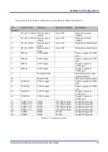
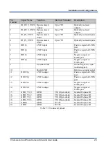
The pinout of each of these connectors is as described in Table 4 and Table 5.
Pin
Number
Signal Name
Function
Electrical Standard
Description
1
IO_OUT_EXT0 Opto-Isolated
output
Up to 70V
Optically isolated
outputs
2
IO_OUT_EXT0 Opto-Isolated
output
Up to 70V
Optically isolated
outputs
3
IO_IN_EXT0
Opto-Isolated
input
Up to 70V
Optically isolated inputs
4
IO_IN_EXT0
Opto-Isolated
input
Up to 70V
Optically isolated inputs
5
RIN1p
LVDS input
Positive signal of LVDS
pair
6
RIN2p
LVDS input
Positive signal of LVDS
pair
7
RIN1n
LVDS input
Negative signal of
LVDS pair
8
RIN2p
LVDS input
Negative signal of
LVDS pair
9
External GND
Ground signal for opto-
isolated signals
10
Board GND
Reference ground signal
11
DOUT1p
LVDS output
Positive signal of LVDS
pair
12
DOUT2p
LVDS output
Positive signal of LVDS
pair
13
DOUT1n
LVDS output
Negative signal of
LVDS pair
14
DOUT2n
LVDS output
Negative signal of
LVDS pair
15
GPIO_5V_0
GPIO
TTL (Open-drain)
General Purpose IO
16
GPIO_5V_2
GPIO
TTL (Open-drain)
General Purpose IO
17
GPIO_5V_1
GPIO
TTL (Open-drain)
General Purpose IO
18
GPIO_5V_3
GPIO
TTL (Open-drain)
General Purpose IO
19
GPIO0
GPIO
LVTTL
General Purpose IO
20
GPIO1
GPIO
LVTTL
General Purpose IO
Table 4: J7 connector pinout
Installation and Configurations


