Copyright © Siemens AG 2010. All rights reserved.
Page
80
ERTEC 400 Manual
Technical data subject to change
Version 1.2.2
7.3.4
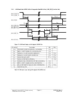
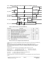
LBU Write to ERTEC 400 with common Read/Write line (LBU_RDY_N active low)
LBU_CS_R_N/
LBU_CS_M_N
LBU_WR_N
LBU_A(20:0)/
LBU_SEG(1:0)/
LBU_BE(1:0)_N
LBU_RDY_N
LBU_D(15:0)
t
WCS
t
ACS
t
CRE
t
CDV
t
CDH
t
CAH
t
CWH
t
RTC
t
RAP
t
WR
Figure 15: LBU Write Sequence with common RD/WR line
Parameter
Description
Min
Max
t
WCS
write signal asserted to chip select setup time
2 ns
1
t
ACS
address valid to chip select asserted setup time
0 ns
t
CRE
chip select asserted to ready enabled delay
5 ns
12 ns
t
CDV
chip select asserted to data valid delay
40 ns
t
RAP
ready active pulse width
17 ns
23 ns
t
CWH
write signal deasserted to chip select deasserted hold time
0 ns
t
CAH
address valid to chip select deasserted hold time
0 ns
t
RTC
ready asserted to chip select deasserted delay
0 ns
t
CDH
data valid/enabled to chip select deasserted hold time
0 ns
t
WR
write recovery time
25 ns
Table 25: LBU write access timing with common Read/Write line
1
The setup time
t
WCS
must be maintained under all circumstances; otherwise the LBU unit drives the ERTEC 400
databus.
The ERTEC 400 has two LBU chip select inputs. One for access to the page configuration register
(LBU_CS_R_N) and one to access to the ERTEC 400 memory address space (LBU_CS_M_N). Only one of
these chip select signals may be active at a time and it is not allowed to chahge the chip select during the
complete access.
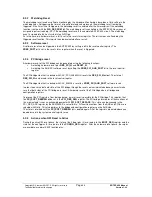
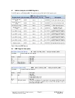
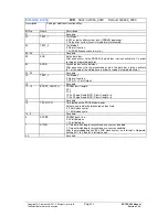
The polarity of the signal LBU_RDY_N can be configured using the input LBU_POL_RDY:
LBU_POL_RDY = 0
(external pull down resistor used)
LBU_RDY_N is LOW active
LBU_POL_RDY = 1
(external pull up resistor used)
LBU_RDY_N is HIGH active
The LBU access control can be configured using the input LBU_CFG:
LBU_CFG = 0
use separate read/write lines (LBU_RD_N and LBU_WR_N)
LBU_CFG = 1
use common read/write lines (LBU_WD_N)
If common read/write line is selected, the unused input LBU_RD_N must be pulled to inactive level with an pull up
resistor.

