Semiconductor Group
10-6
1997-10-01
OTP Memory Operation
C541U
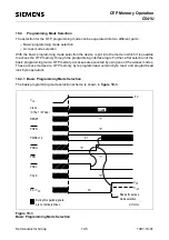
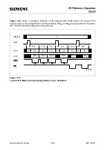
The basic programming mode is selected by executing the following steps :
– With a stable V
DD
a clock signal is applied to the XTAL pins; the RESET pin is set to “1“ level
and the PSEN pin is set to “0“ level.
– PROG, PALE, PMSEL1 and EA/V
PP
are set to “0“ level; PRD, PSEL, and PMSEL0 are set to
“1“ level.
– PSEL is set to from “1“ to “0“ level and thereafter PROG is switched to “1“ level.
– PMSEL1,0 can now be changed; after EA/V
PP
has been set to V
IH
high level or to V
PP
the OTP
memory is ready for access.
The pins RESET and PSEN must stay at “1“ respectively “0“ static signal level during the whole
programming mode. With a falling edge of PSEL the logic state of ALE/PROG and V
PP
(EA) is
internally latched. These two signals are now used as programming write pulse signal (PROG) and
as programming voltage input pin V
PP
. After the falling edge of PSEL, PSEL must stay at “0“ state
during all programming operations.
Note: If protection level 1 to 3 has been programmed (see section 10.6) and the programming mode
has been left, it is no more possible to enter the programming mode !
10.4.2 OTP Memory Access Mode Selection
When the C541U has been put into the programming mode using the basic programming mode
selection, several access modes of the OTP memory programming interface are available. The
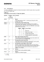
conditions for the different control signals of these access modes are listed in table 10-2.
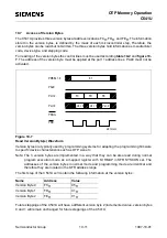
The access modes from the table above are basically selected by setting the two PMSEL1,0 lines
to the required logic level. The PROG and PRD signal are the write and read strobe signal. Data is
transfered via port 0 and addresses are applied to port 2.
The following sections describes the details of the different access modes.
Table 10-2
Access Modes Selection
Access Mode
EA/
V
PP
PROG
PRD
PMSEL
Address
(Port 2)
Data
(Port 0)
1
0
Program OTP memory byte
V
PP
H
H
H
A0-7
A8-15
D0-7
Read OTP memory byte
V
IH
H
Program OTP lock bits
V
PP
H
H
L
–
D1,D0 see
table 3
Read OTP lock bits
V
IH
H
Read OTP version byte
V
IH
H
L
H
Byte addr.
of sign. byte
D0-7
Summary of Contents for C541U
Page 1: ... 8 LW 026 0LFURFRQWUROOHU 8VHU V 0DQXDO http www siem ens d Sem iconductor ...
Page 7: ......
Page 21: ...Semiconductor Group 2 6 1997 10 01 Fundamental Structure C541U ...
Page 37: ...Semiconductor Group 4 6 1997 10 01 External Bus Interface C541U ...
Page 133: ...Semiconductor Group 6 88 1999 04 01 On Chip Peripheral Components C541U ...
Page 163: ...Semiconductor Group 8 8 1997 10 01 Fail Safe Mechanisms C541U ...
Page 185: ...Semiconductor Group 10 14 1997 10 01 OTP Memory Operation C541U ...


