Semiconductor Group
10-9
1997-10-01
OTP Memory Operation
C541U
10.6
Lock Bits Programming / Read
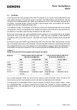
The C541U has two programmable lock bits which, when programmed according tabie 10-3,
provide four levels of protection for the on-chip OTP code memory. The state of the lock bits can
also be read.
Note : A 1 means that the lock bit is unprogrammed. 0 means that lock bit is programmed.
For a OTP verify operation at protection level 1, the C541U must be put into the OTP verification
mode 2.
If a device is programmed with protection level 2 or 3, it is no more possible to verify the OTP
content of a customer rejected (FAR) OTP device.
When a protection level has been activated by programming of the lock bits, the basic programming
mode must be left for activation of the protection mechanisms. This means, after the activation of a
protection level further OTP program/veriry operations are still possible if the basic programming
mode is maintained.
The state of the lock bits can always be read if protection level 0 is selected. If protection level 1 to
3 has been programmed and the programming mode has been left, it is no more possible to enter
the programming mode: In this case, also the lock bits cannot be read anymore.
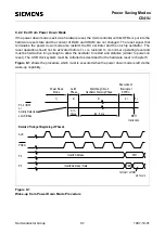
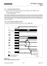
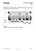
Figure 10-6 shows the waveform of a lock bit write/read access. For a simple drawing, the PROG
pulse is shortened. In reality, for Lock Bit programming, a 100
µ
s PROG low puls must be applied.
Table 10-3
Lock Bit Protection Types
Lock Bits at D1,D0
Protection
Level
Protection Type
D1
D0
1
1
Level 0
The OTP lock feature is disabled. During normal operation of
the C541U, the state of the EA pin is not latched on reset.
1
0
Level 1
During normal operation of the C541U, MOVC instructions
executed from external program memory are disabled from
fetching code bytes from internal memory. EA is sampled and
latched on reset.An OTP memory read operation is only
possible using the OTP verification mode for protection level 1.
Further programming of the OTP memory is disabled
(reprogramming security).
0
1
Level 2
Same as level 1, but also OTP memory read operation using
OTP verification mode is disabled.
0
0
Level 3
Same as level 2; but additionally external code execution by
setting EA=low during normal operation of the C541U is no
more possible.
External code execution, which is initiated by an internal
program (e.g. by an internal jump instruction above the OTP
memory boundary), is still possible.
Summary of Contents for C541U
Page 1: ... 8 LW 026 0LFURFRQWUROOHU 8VHU V 0DQXDO http www siem ens d Sem iconductor ...
Page 7: ......
Page 21: ...Semiconductor Group 2 6 1997 10 01 Fundamental Structure C541U ...
Page 37: ...Semiconductor Group 4 6 1997 10 01 External Bus Interface C541U ...
Page 133: ...Semiconductor Group 6 88 1999 04 01 On Chip Peripheral Components C541U ...
Page 163: ...Semiconductor Group 8 8 1997 10 01 Fail Safe Mechanisms C541U ...
Page 185: ...Semiconductor Group 10 14 1997 10 01 OTP Memory Operation C541U ...

