UX-B20U/UX-B20C/B25C
5 – 14
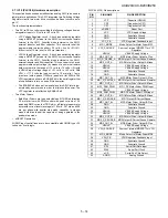
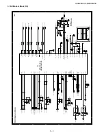
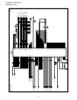
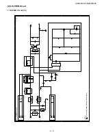
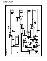
2.7. IC10 (PLCC44) Hardware description
This specfication describes a multifunction analog ASIC to be used in
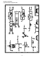
inkjet printer applications. This ASIC integrates two Switching Voltage
Regulator circuits, two motor drive circuits and a Reset circuit in a sin-
gle IC.
The functions implemented are:
• Two DC-to-DC converters providing the following voltages from an
unregulator input of +21 volts to +42 volts DC:
• VCC Voltage Regulator circuit - A buck type switching regulator
using a MOSFET (internal to the ASIC), current sense resistor
(internal to the ASIC), Schottky diode (external to the ASIC),
external inductor and filter capacitor. This converter shall be
programmable to provide 3.3 volts, +5 volts, +5%/-4%,
at a current of 10ma.(min.) to 500 ma.(max./ave.).
• VPH Voltage Regulator circuit - A buck type switching regulator
using a MOSFET (internal to the ASIC), current sense resistor
(internal to the ASIC), Schottky diode (external to the ASIC),
external inductor and filter capacitor. This converter is to have a
programmable output voltage (by means of an external resistor
divider network) in the range of +10 volts to +15 volts, +/2% with
a VBULK input voltage range of +21 volts to +42 volts. With
VPH = +11.75 volts the load current is 10 ma.(min.), 1amp.
(max./ave.) with a peak of 1300 ma. (peak/ave.) for 400 ms. The
VPH regulator shall have a ENABLE bit in the serial register that
allows software to turn on and off this converter.
• The ENABLE bit when set low shall place this ASIC into its low-
est stand-by power mode in order to minimize idle power. The
VCC regulator is not effected by ENABLE bit.
• Two Motor Drivers:
• Both Motor Drivers are to be selectable as EITHER a bidirection
DC motor driver with PWM control with peak currents of 2.0
amps and RMS currents of TBD mA or a Bipolar stepper motor
driver with current levels (average) of 183 ma., 367 ma. and 550
ma. per phase with quarter step mode capability. In stepper
mode both drivers shall be capable of being operated in the
quarter step mode.
• nRESET Generation
All ASIC input control lines are to be compatible with CMOS type +3.3
volts and +5 volts logic.
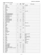
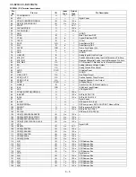
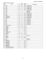
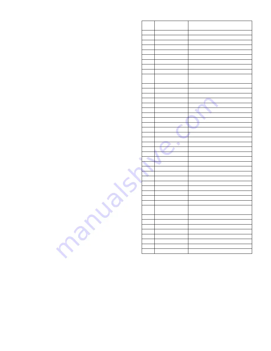
PLCC44 (IC10) Pin descriptions
PIN
NO.
PIN NAME
PIN DESCRPTION
1
VCP
(Capacitor VBULK)
2
CP2
(Capacitor to CP1)
3
CP1
(Capacitor to CP2)
4
nRESET
Reset Port
5
VCC
VCC Supply Voltage
6
GND
Substrate Ground
7
GND
Substrate Ground
8
VCC_FB
VCC Regulator Feedback Input
9
MD1_MODE
Mode Select for Motor Driver MD1
10
VCC_SOURCE
Source of internal MOSFET for VCC
Regulator
11
VBULK
VBULK Supply Voltage
12
MD
MD2-Motor Driver Output a Plus
13
MD_R_SENSE_A
MD2-Output A Current Sense Resistor
14
MD2_OUT_A-
MD2-Motor Driver Output A Minus
15
VBULK
VBULK Supply Voltage
16
VBULK
VBULK Supply Voltage
17
GND
Substrate Ground
18
GND
Substrate Ground
19
MD
MD!-MOtor Driver Output A Plus
20
MD1_R_SENSE_A MD1-Output A Current Sense Resistor
21
MD1_OUT_A-
MD1-Motor Driver Output A Minus
22
MD1_DCM_PWM
MD1_DC Motor Driver PWM Input
23
VBULK
VBULK Supply Voltage
24
MD2_DCM_PWM
MD2-DC Motor Driver PWM Input
25
MD1_OUT_B-
MD1-Motor Driver Output B Minus
26
MD1_R_SENSE_B
MD1-Output B Current Sense
27
MD
MD1-Motor Driver Output B Plus
28
GND
Substrate Ground
29
GND
Substrate Ground
30
VBULK
VBULK Supply Voltage
31
VBULK
VBULK Supply Voltage
32
MD2_OUT_B-
MD2-Motor Driver Output B Minus
33
MD2_R_SENSE_B MD2-Output B Current Sense Resistor
34
MD
MD2-Motor Driver Output B Plus
35
VBULK
VBULK Supply Voltage
36
VPH_SOURCE
Source of internal MOSFET for VPH
Regulator
37
MD2_MODE
Mode Select for Motor Driver MD2
38
VPH_FB
VPH Regulator Feedback Input
39
GND
Substrate Ground
40
GND
Substrate Ground
41
SDI
Serial Port Data Input
42
SCLK
Serial Port Clock
43
nCS
Serial Port Chip Select
44
AGND
Analog Ground
Summary of Contents for UX-B20
Page 2: ... i UX B20U UX B20C B25C ...

