background image

2)

PARTS NAME

PARTS CODE

LOCATION

FFC
CONNECTOR

QCNCW7217RC3J

TOUCH
PWB: CN1

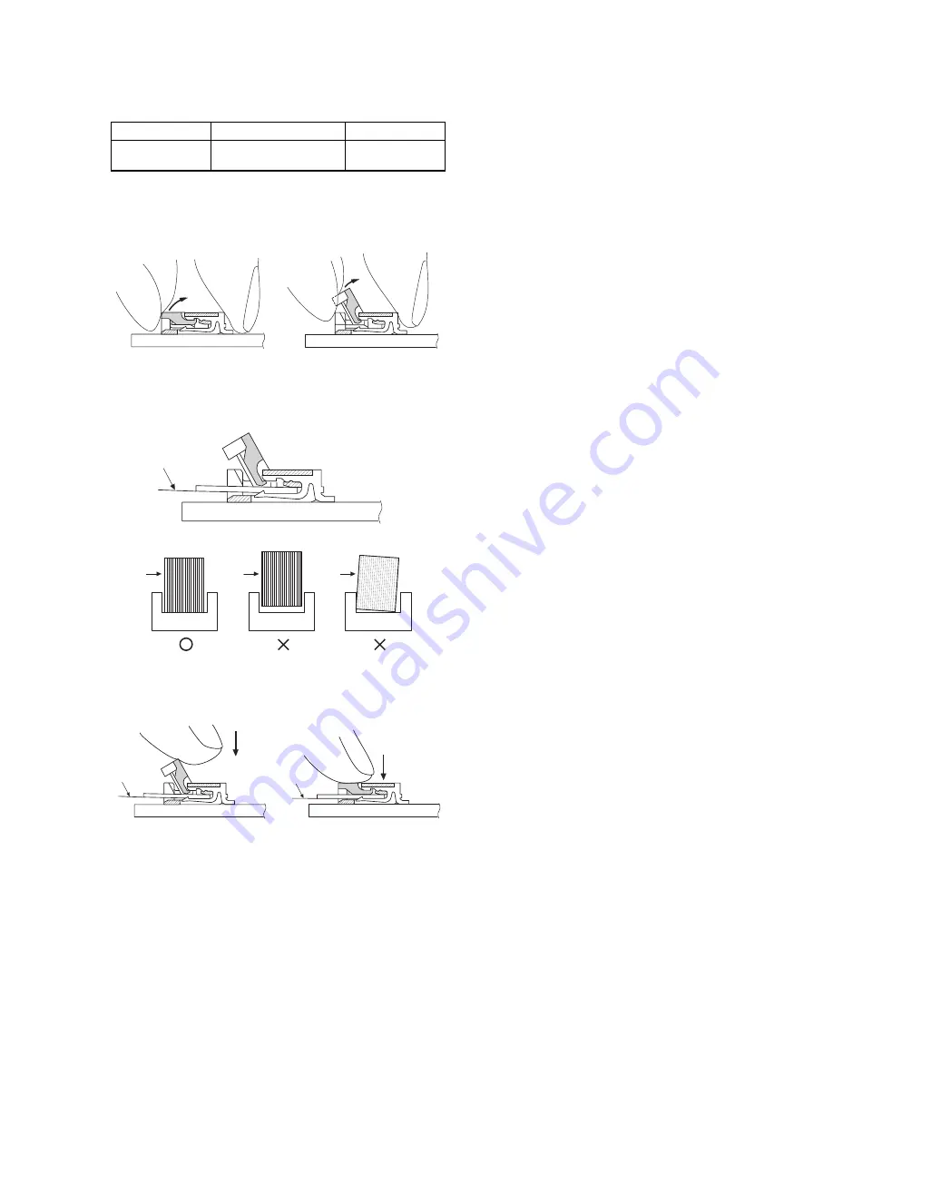
How to Insert FFC

(1)

Open the slider to unlock position
Open the slider upwards up to an angle of 60 degrees. If the
slider does not fully open, the FFC can not be smoothly inserted.

(2)

Insert the FFC
Insert the FFC firmly until the FFC hits the bottom of the
connector’s insulator.

(3)

Close the slider to lock position

Insert the FFC and then push the slider downward.

(4)

To pull out the FFC, unlock the slider to pull it out in the same
procedures as (1).

9. Note for handling Rear Display PWB

unit

SYSTEM RESET is controlled by the battery-protected CKDC9 (1
chip microcomputer) on the rear display PWB. RESET control be-
comes impossible if the connection cable leading to the MAIN PWB.

Don’t disconnect the CABLE when repairing and adding OPTION.

If it is needed to disconnect the CABLE or it is disconnected by
mistake, connect again and carry out SRV RESET.

FFC

FFC

CONNECTOR

FFC

CONNECTOR

FFC

CONNECTOR

FFC

FFC

3 – 8

Summary of Contents for UP-3300

Page 1: ...e set This document has been published to be used for after sales service only The contents are subject to change without notice CHAPTER 1 SPECIFICATIONS 1 1 CHAPTER 2 OPTIONS 2 1 CHAPTER 3 SERVICE PRECAUTION 3 1 CHAPTER 4 PROGRAM RESET and SRV mode 4 1 CHAPTER 5 MASTER RESET All Memory Clear 5 1 CHAPTER 6 DIAGNOSTICS SPECIFICATIONS 6 1 CHAPTER 7 CIRCUIT DESCRIPTION 7 1 CHAPTER 8 CIRCUIT DIAGRAM 8...

Page 2: ...BATTERY DISPOSAL Contains Nickel Metal Hydride Battery Must be Disposed of Properly Contact Local Environmental Officials for Disposal Instructions ...

Page 3: ...l The operations can be performed by touching the screen that shows keys or items in the receipt window of the operator display 1 Operator display touch panel 3 1 Display 1 Front display ITEM SPECIFICATIONS NOTE Type DSTN color LCD with back light With 256 colors Screen size 10 4 Full screen Dot format 640 W 480 H mm Full dot Dot size 0 09 RGB W 0 31 mm Dot space 0 02 mm Note that the application ...

Page 4: ...items and media types Receipt ON OFF status indicator R Appears when the receipt ON OFF function is set to OFF The indication disappears when the function signs ON PLU level shift indicator L01 L10 Shows the PLU level currently selected Price level shift indicator P1 P7 Indicates the PLU price level currently selected Sentinel mark X Appears in the lower right corner of the screen when the cash in...

Page 5: ...Condi GLU ENTER Dept 01 Dept 02 Dept 03 Dept 04 NBAL AUTO NORMAL L1 MEDIUM L2 SUB SUB1 TEXT FNC 13 PAYMEN FNC 11 DRINKS MENUE1 DRINKS MENUE2 DRINKS MENUE3 DRINKS MENUE4 MODE VATSFT DRINKS MENUE5 DRINKS MENUE6 Light Beer Light Beer Mineral water Light Beer Fanta Light Beer Coke Light Beer Light Beer DAILY MENUE2 COND MGR FNC 12 MORE VOID CANCEL CLEAR 4 7 1 0 5 8 2 MORE 6 9 3 Next Condi GLU ENTER De...

Page 6: ...xt Condi GLU ENTER NBAL TEXT FNC 13 TEXT FNC 14 PAYMEN FNC 11 START MENUE 10 FISH MENUE 11 MEAT MENUE 12 DESS MENUE 13 HOME VATSFT KEY19 KEY20 KEY21 KEY22 KEY23 KEY24 KEY25 KEY26 KEY27 KEY28 KEY29 KEY30 SPECIALITIES MENUE14 CHICKEN MENUE 15 SUB SUB1 P2 Pint Auto key AUTO MGR FNC 12 MORE VOID CANCEL CLEAR 4 7 1 0 5 8 2 MORE 6 9 3 Next Condi GLU ENTER NBAL TEXT FNC 13 TEXT FNC 14 PAYMEN FNC 11 START...

Page 7: ...4 AUTO23 AUTO22 AUTO21 AUTO20 AUTO19 AUTO18 CANCEL MGR FNC 12 VOID RA PO CANCEL CLEAR 4 7 1 0 5 8 2 6 9 3 GLU ENTER NBAL ST VOID GC RCPT Entertain ment HOME VATSFT DEDUCTION CREDIT 3 DEDUCTION DEPOSIT EXCHANGE 1 DEPOSIT EXCHANGE 2 H TRANS CREDIT 2 NC TIP CREDIT 1 CASH TIP CHECK CASH TL SUB TOTAL BILL Transfer BILL Separate 00 AUTO 4 7 1 0 5 8 2 6 9 3 00 P DOWN P UP EMPL CLK VOID MGR AUTO22 AUTO21 ...

Page 8: ...CASH2 Used to enter the cash 2 payment CHK thru CHK4 Used to enter the check payment check 1 thru 4 Caption default Function CR1 thru CR8 Used to enter the credit sale credit 1 thru 8 EXCHANGE1 to EXCHANGE9 Used to creates a subtotal in foreign currency exchange 1 thru 9 OPEN THE TABLE Used to lookup the guest check OPEN THE CAR Used to lookup the guest check for drive thru function NBAL Used to o...

Page 9: ...ax 10 clerks WMF clerk keys max 127 clerks The standard POS terminal has been shipped with the real clerk key system being programmed If you want to change the clerk identifica tion system contact your authorized SHARP dealer Real clerk keys 1 2 3 4 5 and 6 These keys serve to identify clerks Put one of the 1 through 6 keys in the clerk switch Clerk code entry 1 through 9999 Enter the clerk code b...

Page 10: ...cale Local xxxxxxx CAT Local xxxxxxx RS 232 R J Printer Option ER 01PU IR MCR Option UP E12MR2 Poll Display Option UP P16DP NEW NEW NEW NEW NEW RS 232 Board Option ER A7RS XXX 2 Max 6point EFT VF Board Option ER 02EF Mastermachine SRN Remote Drawer Option ER 03DW 04DW 05DW XXXXXX memory board Option UP P02MB2 XXXX Printer Option UP T80BP xxxxxxxxxx IR Communication 1 System configuration 2 1 ...

Page 11: ...r UP E12MR2 for ISO 1 2 stripe card EFT terminal I F ER 02EF 3 Local purchase options No COMPONENT NAME MODEL NAME 1 External printer TM T85 T88 2 Slip printer TM U295 TM H5000 3 Scale I F 4 Drink Dispensor 4 Service options No NAME PARTS CODE DESCRIPTION 1 1 hole clerk key The key No 1 to No 6 ore supplied together with UP 5700 LKGIM1004BH07 Key No 7 LKGIM1004BH08 Key No 8 LKGIM1004BH09 Key No 9 ...

Page 12: ...y No 52 LKGIM1004BH53 Key No 53 LKGIM1004BH54 Key No 54 LKGIM1004BH55 Key No 55 LKGIM1004BH56 Key No 56 LKGIM1004BH57 Key No 57 LKGIM1004BH58 Key No 58 LKGIM1004BH59 Key No 59 LKGIM1004BH60 Key No 60 LKGIM1004BH61 Key No 61 LKGIM1004BH62 Key No 62 LKGIM1004BH63 Key No 63 LKGIM1004BH64 Key No 64 LKGIM1004BH65 Key No 65 LKGIM1004BH66 Key No 66 LKGIM1004BH67 Key No 67 LKGIM1004BH68 Key No 68 LKGIM100...

Page 13: ...Key No 107 LKGIM1004BHA8 Key No 108 LKGIM1004BHA9 Key No 109 LKGIM1004BHA0 Key No 110 LKGIM1004BHB1 Key No 111 LKGIM1004BHB2 Key No 112 LKGIM1004BHB3 Key No 113 LKGIM1004BHB4 Key No 114 LKGIM1004BHB5 Key No 115 LKGIM1004BHB6 Key No 116 LKGIM1004BHB7 Key No 117 LKGIM1004BHB8 Key No 118 LKGIM1004BHB9 Key No 119 LKGIM1004BHB0 Key No 120 LKGIM1004BHC1 Key No 121 LKGIM1004BHC2 Key No 122 LKGIM1004BHC3 ...

Page 14: ...n view Connection diagram 5 2 MCR test card UKOG 6718RCZZ Used when executing the diagnostics of the UP E12MR2 External view Test pins Used to check the bus signals Bus connector Used to check the bus signals Connected to the UP 3300 Mother PWB UP 3300 bus connector ER A7RS 2 5 ...

Page 15: ...tion The coordinates on the touch panel and those on the VGA display may not match for the following reasons The physical deviation between the touch panel and display Variations in electric resistance coordinate conversion on the touch panel Correction of such a deviation is called calibration 2 Timing of starting calibration Calibration is started at the following two cases SRV reset MRS 1 When ...

Page 16: ...ction points 393 402 2080 402 3767 402 393 2048 2080 2048 3767 2048 393 3697 2080 3697 3767 3697 7 Step 6 is repeated for the nine correction points Correction is performed in an arbitrary order At first all of the nine points are displayed in white and they turn black as corrected 8 After all of the points are corrected the command correction mode end is issued to the controller The maximum coord...

Page 17: ...he ER A7RS Master ROM 1 VHI27801RAFxx Master ROM 2 VHI27801RAGxx 2 IPL sitch on the ER A7RS Set the IPL SW to ON position 3 Install the ER A7RS to the UP 3300 The UP 3300 power should be turned OFF 4 Turned on the power of the UP 3300 5 The buzzer sounds intermittently during the running of IPL and the program finishes after the buzzer gives five beeps at short inter vals 6 Turn OFF the power of t...

Page 18: ...ame of S type ROM object 8 Program data is sent to UP 3300 automatically 8 Program data is received from P C automatically UP 3300 shows 9 UTL33 EXE is completed P C shows Completed 9 UP 3300 shows Completed 10 Turn OFF the power 11 Select Normal Mode Set IPL switch to OFF 12 Execute Service Reset on UP 3300 IPL SW ON IR Filter IPL from IR IPL from IR Connected IRDA 115200 21 22 23 24 25 26 27 28 ...

Page 19: ...it Map image 9 Program data is sent to UP 3300 automatically 9 Program data is received from P C automatically 10 UTL33 EXE is completed P C shows Completed 10 ER 3300 shows Completed And UP T80BP prints out the LOGO image 11 Touch OK button 12 Touch EXIT button 13 Turn OFF the power of UP 3300 14 Execute Master Reset on UP T80BP 4 3 UP T80BP IPL No Procedure on P C side No Procedure on UP 3300 si...

Page 20: ...it 1 of DipSwitch 2 to OFF to enter Nomal Mode 17 Execute Master Reset on UP T80BP UP T80BP Utility EXIT UP T80BP Utility EXIT IPL mode IPL mode UP T80BP Utility E X I T Complete OK Usage of UTL33 EXE UTL33 EXE is a utility program on P C a program that sends the application program data of UP 3300 the image data of the Logo stamp of UP T80BP or the application program data of UP T80BP in order to...

Page 21: ...the air groove away from water and oil Input is performed with fingers Do not use a hard thing for input ting 7 Note for handling of LCD The LCD elements are made of glass BE careful not to give them strong mechanical shock or they may be broken Use extreme care not to break them If the LCD element is broken and the liquid is leaked do not lick it If the liquid is attached to your skin or cloth im...

Page 22: ... Insert the FFC and then push the slider downward 4 To pull out the FFC unlock the slider to pull it out in the same procedures as 1 9 Note for handling Rear Display PWB unit SYSTEM RESET is controlled by the battery protected CKDC9 1 chip microcomputer on the rear display PWB RESET control be comes impossible if the connection cable leading to the MAIN PWB Don t disconnect the CABLE when repairin...

Page 23: ...ed to return the machine back to its operation state after a lock up has occured PROCEDURE 1 Turn off the AC switch 2 Set the reset switch to ON position 3 Turn on the AC switch 4 Set the reset switch to OFF position 5 The reset menu windowis displayed as shown below DISPLAY Touch the PROGRAM RESET key 6 PROGRAM RESET is started 7 After completion of the program reset the SRV mode is displayed as ...

Page 24: ...mber for MRS 1 11111111 8 MASTER RESET 1 is started DISPLAY 9 After completion of the master reset the buzzer sounds three times and the following SRV mode display is shown DISPLAY SRV mode screen 2 MRS 2 Master resetting 2 Clear the entire memory and resumes initial values The keyboard must be entered by hand This reset is used if an application needs different kyeboard layout other than that sup...

Page 25: ...22222 8 Set the fixed keys in the table below Start from the HOME key The key are displayed sequentially DISPLAY No KEY NAME 1 HOME 2 CANCEL 3 CL 4 MODE 5 UP 6 DOWN 9 MASTER RESET 2 is started DISPLAY 10 After completion of the master reset the buzzer sounds three times and the following SRV mode display is shown DISPLAY SRV mode screen Please select MASTER RESET MASTER RESET 2 ENTER PASSWORD ENTE...

Page 26: ... configuration 2 1 Test system UP 3300 only 3 Diagnostics Starting the diagnostics This diagnostics program is written in the external ROM and executed by the CPU H8 510 To operate this program the following condi tions must be satisfied 1 The power for the logic system is proper 5V VRAM VCKDC POFF 20V 2 The input output pins and the internal logic of the CPU are normal In addition CKDC9 MPCA8 the...

Page 27: ...ss and the bit are displayed only when the error occurs If the error does not occur the error address will not be displayed 3 Terminating procedure After completion of check press the Touch panel 2 UP P02MB2 Check 1 Check content The UP P02MB2 presence check is performed in the following procedure The memory contents will not be changed by this check 55AAH is written into 9FFFFEH 9FFFFEH is read a...

Page 28: ...t 0PAGE where the IPL is stored is individually controlled 2 Display Standard ROM Sum Check PASS or ERROR IPL PROGRAM Version APL PROGRAM Version 27801R UP 3300 27801R UP 3300 Display the version BLOCK Version 20 21 22 23 24 25 26 27 28 29 2A 2B 2C 2D 2E 2F 30 31 32 33 34 35 36 37 38 39 3A 3B 3C 3D 3E 3F 3 Terminating procedure After displaying the check result press the Touch panel to ter minate ...

Page 29: ... The main PWB and the option PWB RS232 interface of ER A7RS are checked Attach the 9 pin D Sub loop back connector UKOG 6717RCZZ of wiring in Fig 3 11 Fig 3 11 Wiring diagram of loop back connector UKOG 6717RCZZ The following menu is displayed Press the touch key for the opera tion you want to execute to execute individual Diag programs Pressing the CANCEL key returns the screen to the Diag MAIN m...

Page 30: ...256 bytes of 00H 0FFH are used for data transfer check The baud rate is set to 38400BPS Timer check RS232 on board timer Before performing the check set the timer to TCVDT start and 5ms Then perform the following procedure During execution of the check TRQ must not be generated After 5ms from completion of the check TRQ must be generated 2 Display RS232 CH1 Check ER DR ERROR All the contents of an...

Page 31: ... left to right of the screen viii 16 color bars are displayed from left black blue green cyan red magenta brown white gray light blue light green light cyan light red light magenta light yellow and light white ix The outermost peripheral of the LCD s active area is dis played in one dot line White rester test x H pattern H is displayed in 80 digits and 25 lines The 15th line only has 39 digits of ...

Page 32: ...OFF shows carrier ON b2 An interruption of CTC CH2 or CH3 cannot be made Timer interruption b1 ROM sum check error b0 TAM error Execute diagnostics command 1 The error status is displayed The error status is as shown in the table below b7 An error is generated The error print is always 1 b6 An unexpected interruption is generated b5 DMA sent data and received data are different b4 The number of da...

Page 33: ... of one master machine and max 15 satellite machines Note for starting the check When checking the set in which the SRN setting has been made cancel the SRN setting before starting this check When checking the actually composed system disconnect the SRN cables of the sets which are not checked or cancel the SRN setting If it is set to SRN exits data may be destroyed The transmission check setting ...

Page 34: ...The error code is displayed The error codes are as shown below 01 Command abnormality except for during transmission 02 No data received 03 Received data present Received data remained 04 Remote station not ready in sending NTDY is sent back because the remote station is not ready for reception 05 Reception buffer full in sending The controller reception buffer of the remote machine is full 06 Res...

Page 35: ...ting procedure Press the Touch panel to terminate the check 4 Data Transmission Check Send mode 1 Check content Continuous IR communication between the UP 3300 and the UP 3300 This mode is on the transmission side When data of 256byte 00H 0FFH are transmitted the data packet counter is incremented by one Check that the counter increments 2 Display Data Transmission Check Send MODE COUNTER The RING...

Page 36: ... only and the following LOOP BACK Connectors are required Fig 3 11 Wiring diagram of loopback connectors UKOG 2356BHZZ 2 Indication The indication is the same as that for RS232 DIAGNOSTICS 3 End Press the PANEL to end the program 2 Printer Print Check 1 Check Send the signal to generate a receipt by DIAG COMMAND to the UP T80BP 3 14 EFT ER 02EF Diagnostics 1 Procedure 1 Select EFT Diag in the DIAG...

Page 37: ...8 IR PSEUDO SRAM 1MB OPC2 EXT SLOT 80pin x 2 RAMCN 72pin CKDC9 SW VCC LCD 640 x 480 dots DRIVER 24V DRIVER 24V DRIVER RECEIVER VGA CONTROLLER MN89303A BRIGHTNESS CONTROL VOLUME INVERTER CONTRAST ADJUSTMENT VOLUME POWER SUPPLY VRAM DRAM 512K SRN FLASH ROM 2MB PRINTER TOUCH PANEL CONTROLLER 7 1 ...

Page 38: ...IRQ2 IRQ1 IRQ0 VCC AVCC P73 P72 112 111 110 109 108 107 106 105 104 103 102 101 100 99 98 97 96 95 94 93 92 91 90 89 88 87 86 85 P41 P42 P43 P44 P45 P46 P47 VSS P50 P51 P52 P53 P54 P56 P57 P60 P61 P62 P63 P64 P65 P66 P67 VSS AVSS P70 P71 57 58 59 60 61 62 63 64 65 66 67 68 69 70 71 72 73 74 75 76 77 78 78 80 81 82 83 84 A8 A9 A10 A11 A12 A13 A14 A15 VSS A16 A17 A18 A19 A20 A21 A22 A23 VSS P30 WAIT...

Page 39: ...7 P16 P15 P14 P13 P12 P11 P10 D15 D14 D13 D12 D11 D10 D9 D8 P57 P56 P55 P54 P53 P52 P51 P50 P67 P66 P65 P64 P63 P62 P61 P60 P73 P72 P71 P70 TXD2 RXD2 TXD1 RXD1 SCK2 IRQ3 SCK1 IRQ2 IRQ1 IRQ0 H8 500 CPU DTC Serial communication interface x 2ch 8bit timer 16bit free running timer x 2ch Refresh controller Wait state controller A D convertor Interruption controller Clock oscillator Watch dog timer Data...

Page 40: ... In 5V 56 P40 VCC In 5V 57 P41 GND In GND 58 P42 GND In GND Pin No Symbol Signal name In Out Function 59 P43 GND In GND 60 P44 MCRINT In MCR interrupt signal 61 P45 GND In GND 62 P46 SHEN In CKDC interface shift enable signal 63 P47 GND In GND 64 VSS GND In GND 65 P50 GND In GND 66 P51 GND In GND 67 P52 GND In GND 68 P53 GND In GND 69 P54 GND In GND 70 P55 GND In GND 71 P56 GND In GND 72 P57 STOP ...

Page 41: ... DT2 129 DT3 128 DT4 127 RJTMG 126 TPCKI 125 TPTXD 124 RAS2 123 ROS2Z 122 ROS1Z 121 OPTCSZ 41 ID3 42 GND 43 ID4 44 ID5 45 ID6 46 ID7 47 SSPRQZ 48 RESETZ 49 INT2Z 50 INT3Z 51 RXDI 52 TXDI 53 SCKI 54 IRQ0Z 55 A0 56 A1 57 A2 58 A3 59 A4 60 A5 61 GND 62 VDD 63 A6 64 A7 65 A8 66 A9 67 A10 68 A11 69 A12 70 A13 71 A14 72 A15 73 A16 74 A17 75 A18 76 A19 77 A20 78 A21 79 A22 80 LCDCZ 120 EXINT0Z 119 EXINT1...

Page 42: ...RDD1 CLS2 RCP2 RDD2 TPTRDYZ TPTXD TPRXD TPCKI TPRDY TPRRDYZ SSPRQZ DAX2 TXDI SCKI RXDI DAX1 SCK1 STH2 HTS2 SCK2 STH2 HTS1 INT1Z INT2Z INT3Z EXINT0Z EXINT1Z EXINT2Z INT4Z TESTZ TEST0 TEST1 TEST2 MD0 MD1 IRQ02 EXINT3Z DECODE BUFFER READ WRITE CONTROL WAIT CONTREOL MCR I F USART X2 TOUCH PANEL I F USART SSP COMPARISON REGISTER BAR IR CONTROL SERIAL CHANNEL SELECT for CKDC INT CONTROL TEST LOGIC M P C...

Page 43: ...6 IO DATA BUS 46 ID7 IO DATA BUS 47 SSPRQZ O SSP REQUEST FOR CPU 48 RESETZ ICS MPCA RESET 49 INT2Z ICU INTERRUPT INPUT TPRRDY Pin No Name I O Description 50 INT3Z ICU INTERRUPT INPUT TPTRDY 51 RXDI O SERIAL OUT FOR CPU 52 TXDI IS SERIAL IN FROM CPU 53 SCKI IU SERIAL CLOCK FROM CPU 54 IRQ0Z O INTERRUPT SIGNAL FOR CPU 55 A0 I ADDRESS BUS 56 A1 I ADDRESS BUS 57 A2 I ADDRESS BUS 58 A3 I ADDRESS BUS 59...

Page 44: ...INTERFACE 128 DT4 ON NU 129 DT3 ON NU 130 DT2 ON NU 131 DT1 ON NU 132 GND 133 DT7 ON NU 134 DT6 ON NU 135 DT5 ON NU 136 RJMTS ON NU 137 RJMTD ON NU 138 DT9 ON NU 139 DT8 ON NU 140 SYNC IU NU 141 ASKRXZ ICS IR INPUT FROM IR UNIT 142 VDD 143 GND 144 RDD1 ICS SERIAL IN FROM MCR TRACK1 145 RAS3 O NU 146 CLS1 ICS CARD SENSE ON MCR TRACK1 147 SLMTD ON NU Pin No Name I O Description 148 SLMTS ON NU 149 R...

Page 45: ... 134 RTSC 133 DTRC 132 TRNDTC 131 CSC 130 GND 129 SYCBKB 128 TRNEMPB 127 RCVRDYB 126 TRNRDYB 125 DSRB 124 CTSB 123 RCVDTB 122 RTSB 121 DTRB 41 CI2 42 CS2 43 CD3 44 BRK3 45 TRNEMP3 46 RCVRDY3 47 TRNRDY3 48 CTS3 49 RCVDT3 50 CI3 51 CS3 52 D0 53 D1 54 D2 55 D3 56 GND 57 D4 58 D5 59 D6 60 D7 61 GND 62 VCC 63 X1 64 X2 65 XOUT 66 TRCK 67 AB0 68 AB1 69 US1CH 70 PX 71 POF 72 RSRQ 73 TRV 74 RXDATA0 75 TXE ...

Page 46: ...send signal 19 RCVDT0 RCVDT1 IS RS 232 reception data signal 20 VCC VCC 5V 21 GND GND GND 22 CI0 CI1 IS RS 232 control signal CI input 23 RTS0 RTS1 O RS 232 request to send signal Pin NO Name UP 3300 I O Description 24 CS0 CS1 O RS 232 chip select signal 25 CD1 DCD2 IS RS 232 control signal CD input 26 BRK1 BRK2 IS RS 232 break signal 27 TRNEMP1 TRENMP2 IS RS 232 transmission buffer empty signal 2...

Page 47: ...nal from CPU 89 DB0 DB0 IO DATA BUS USART Pin NO Name UP 3300 I O Description 90 DB1 DB1 IO DATA BUS USART 91 DB2 DB2 IO DATA BUS USART 92 DB3 DB3 IO DATA BUS USART 93 GND GND GND 94 DB4 DB4 IO DATA BUS USART 95 DB5 DB5 IO DATA BUS USART 96 DB6 DB6 IO DATA BUS USART 97 DB7 DB7 IO DATA BUS USART 98 R RDH O Read signal to USART 99 W WRH O Write signal to USART 100 VCC VCC 5V 101 GND GND GND 102 RES ...

Page 48: ...2 4 Z80 CPU 1 Features The extensive instruction set contains 158 instructions including the 8080A instruction set as a subset NMOS version for low cost high performance solutions CMOS version for high performance low power designs Z0840006 6 17 MHz CMOS Z84C0006 DC to 6 17 MHz Z84C008 DC to 8 MHz Z84C0010 DC to 10 MHz Z84C0020 DC 20 MHz 6 MHz version can be operated at 6 144 MHz clock The Z80 mic...

Page 49: ...SRQ In Bus request signal 23 RESET S RES In Reset signal 24 M1 S M1 Out Machine cycle one signal 25 RFSH NC NC 26 GND GND GND 27 A0 S A0 Out Address bus 28 A1 S A1 Out Address bus 29 A2 S A2 Out Address bus 30 A3 S A3 Out Address bus 31 A4 S A4 Out Address bus 32 A5 S A5 Out Address bus 33 NC NC NC 34 A6 S A6 Out Address bus 35 A7 S A7 Out Address bus 36 A8 S A8 Out Address bus 37 A9 S A9 Out Addr...

Page 50: ...gral multiple of the clock period the prescaler value 16 or 256 and the time constant that is preset in the down counter A timer is triggered automatically when its time con stant value is programmed or by an external CLK TRG input Three channels have two outputs that occur at zero count The first output is a zero count timeout pulse at the ZC TO output The fourth channel Channel 3 does not have a...

Page 51: ...n configuration Pin No Symbol Signal name In Out Function 1 READY READY In Ready signal 2 HLDAK HLDAK In Hold acknowledge signal 3 ASTB S ASTB Out Address strobe signal 4 AEN S AEN Out Address enable signal 5 HLDRQ HLDRQ Out Hold request signal 6 NC NC NC 7 CS CS In Chip select signal 8 CLK CLK In Clock 9 RESET SRNRESET In Reset signal 10 DMAAK2 S DACK2 Out DMA acknowlidge signal 11 DMAAK3 S DACK3...

Page 52: ...ontrol circuit The transmission control circuit is divided into the modem unit carrier detect unit collision detect unit Fig 6 a Modem circuit The transmission data input from the ADLC are PE modulated phase encoding modulation the circuit to be output to the transmission driver and the reception data input from the trans mission receiver are demodulated and produced at the ADLC b Collision detect...

Page 53: ...b 43 DRQWS Sub Out DMA request write to sub 44 RDH Host In Read from Host 45 WRH Host In write from Host 46 INTH Host Out Interrupt to host 47 DAK Host In DMA acknowledge from host 48 TCH Host In Terminal count from host 49 DRQWH Host Out DMA request read to host 50 DRQWH Host Out DMA request write to host 51 CS Host In Chip select from host 52 VSS GND 53 N U 54 DB0 Host I O Data bus 55 DB1 Host I...

Page 54: ... SD5 49 SD4 50 SD3 51 SD2 52 SD1 53 SD0 54 GND 55 VDD 56 IOCHRDY 57 MEMCS16 58 IOCS16 59 GND 60 VDD 61 DCLK 62 DISP 63 LP 64 FP GND SA18 BIOSEN REFRESH 96 MA1 95 MA2 94 MA3 93 MA4 92 MA5 91 MA6 90 MA7 89 MA8 88 MA9 87 VDD 86 GND 85 84 LCDON 83 BACKON 82 LD0 81 LD1 80 LD2 79 LD3 78 LD4 77 LD5 76 LD6 75 LD7 74 VDD 73 GND 72 UD0 71 UD1 70 UD2 69 UD3 68 UD4 67 UD5 66 65 LOGICON UD6 UD7 1 XIN RESET TES...

Page 55: ... 60 VDD VCC In 5V 61 DCLK XCK Out Data shift clock 62 DISP DISP Out Display enable 63 LP LP Out Line pulse 64 FP YD OUt Frame pulse 65 UD7 DU7 Out Upper data 66 UD6 DU6 Out Upper data 67 UD5 DU5 Out Upper data 68 UD4 DU4 Out Upper data 69 UD3 DU3 Out Upper data 70 UD2 DU2 Out Upper data 71 UD1 DU1 Out Upper data 72 UD0 DU0 Out Upper data 73 GND GND In GND 74 VDD VCC In 5V 75 LD7 DL7 Out Lower data...

Page 56: ... and counter overflow 2 Pin description Pin No Symbol Signal name In Out Function 1 SB SB Out Segment B 2 SC SC Out Segment C 3 SD SD Out Segment D 4 SE SE Out Segment E 5 SF SF Out Segment F 6 SG SG Out Segment G 7 P4 AP Out 8 P0 NC NC 9 P1 NC NC 10 P2 DP Out Decimal point 11 P3 ID Out Indicator Pin No Symbol Signal name In Out Function 12 MODR VCC 5V 13 CFSR CFSR In Clerk key Feed key Switch ret...

Page 57: ...t EXTENDED PSRAM2 DECODE EVEN 900000H 9FFFFFH 23 IPLON0 In IPL SIGNAL 24 PSRF0 Out PSRAM REFRESH 25 OWR Out PSRAM WRITE ODD SIDE 26 M3SWP Out MODE3 BUS SWAP FOR PSRAM ACCESS WHEN IPL 27 Y2 SCLK ISP 28 VCC 29 Y1 RESET ISP 30 MODE ISP Pin No Name I O Function 31 RASPN2E In EXTENDED PSRAM2 DECODE FROM MPCA 800000H 9FFFFFH 32 RASPN2 In EXTENDED PSRAM2 DECODE FROM MPCA 800000H 9FFFFFH 33 RASPN12 In PSR...

Page 58: ...nal I O area is used for peripheral modules outside the CPU For more information refer to the H8 510 hardware manual and peripheral device specification 00FE80h 00FF80h 00FFA0h 00FFB0h 00FFB4h 00FFB8h 00FFBCh 00FFC0h 00FFD0h 00FFE0h 00FFF0h 00FFFFh Internal I O area MPCCS MCR1Z MCR2Z OPCCS2 OPCCS1 T PZ Not used OPTCSZ Expanded MPC not used PRNZ not used CPCSZ not used TPRCI not used CPCSZ is CPC s...

Page 59: ...D by setting the expanded function control register bit5 of MN89303A to H with software The LCD screen isn t turned on until 5V is sup plied 4 5 Back light control The back light is turned ON OFF by the MN89303A terminal BACK ON The initial value is L and the back light is off By setting the expanded function control register bit6 of MN89303A to H the in verter unit is turned on 4 6 Luminance and ...

Page 60: ...fly explained below The gate array always compares the break address register BAR built in the gate array with the address bus to monitor the address bus If both agree the gate array outputs the NMI signal to the CPU which in turn shifts from normal handling to exception handling In both the MPCA7 and the MPCA8 SSP is achieved by the above operation The setting of the break address register BAR is...

Page 61: ...terface The expanded RAM connector terminals are shown in the table The 72 pin S O DIMM is used for the connector Extension RAM connector terminals ADDRESS DECODER RAS ROS IO X3 WAIT ENABLE REGS ENABLE 1WAIT 2WAIT 3WAIT WAIT PULSE GENERATOR ADDRESS DATA WAIT CONTROL REGS EXWAITZ VWAITZ S E L E C T E R WAITZ 00FF8Dh 00FF8Fh DATA TXD2 P87 SCK2 P83 RXD2 P84 IRQ0 RES STOP P57 FT12 HTS SCK STH TXD1 SCL...

Page 62: ...tional drawer P35 DR1 Drawer 2 optional drawer P36 DR2 Reserved P37 DR3 Reserved One port corresponds to one drawer Theoretically it is possible to drive multiple drawers at the same time but this processing must be inhibited softwarewisely because of power supply capacity and driver hardware factors If a power failure is detected the drawer solenoid drive must be stopped as soon as possible The d...

Page 63: ...iming of the MCR interface signals is given below 1 Example of timing 2 Detailed timing relation between DATA and CLOCK PULSE The NULL CODE is basically written prior to the opening code The opening code detection algorithm is considered because data may become corrupt before and after the CARD detection signal due to a worn magnet stripe 19 Touch panel interface The 8251 built in the MPCA8 is use...

Page 64: ...7 P 6 5 7 8 P 6 6 7 9 P 6 7 8 0 V S S 8 1 A V S S 8 2 P 7 0 8 3 P 7 1 8 4 P 7 2 8 5 P 7 3 8 6 A V C C 8 7 V C C 8 8 I R Q 0 8 9 I R Q 1 9 0 S C K 1 I R Q 2 9 1 S C K 2 I R Q 3 9 2 R X D 1 9 3 T X D 1 9 4 R X D 2 9 5 T X D 2 9 6 V S S 9 7 E X T A L 9 8 X T A L 9 9 V S S 1 0 0 X 1 0 1 E 1 0 2 A S 1 0 3 R D 1 0 4 H W R 1 0 5 L W R 1 0 6 R F S H 1 0 7 V C C 1 0 8 M D 0 1 0 9 M D 1 1 1 0 M D 2 1 1 1 S ...

Page 65: ... 0 7 2 G N D 7 3 V D D 7 4 L D 7 7 5 L D 6 7 6 L D 5 7 7 L D 4 7 8 L D 3 7 9 L D 2 8 0 L D 1 8 1 L D 0 8 2 B A C K O N 8 3 L C D O N 8 4 L O G I C O N 8 5 G N D 8 6 V D D 8 7 M A 9 8 8 M A 8 8 9 M A 7 9 0 M A 6 9 1 M A 5 9 2 M A 4 9 3 M A 3 9 4 M A 2 9 5 M A 1 9 6 M A 0 9 7 G N D 9 8 V D D 9 9 R A S 1 0 0 U C A S 1 0 1 L C A S 1 0 2 W E 1 0 3 M D 1 5 1 0 4 M D 1 4 1 0 5 M D 1 3 1 0 6 M D 1 2 1 0 7...

Page 66: ...1 0 1 8 A 1 1 1 7 A 1 2 1 3 A 1 3 1 2 A 1 4 1 1 A 1 5 1 0 A 1 6 8 A 1 7 7 A 1 8 6 A 1 9 5 A 2 0 4 C E 0 1 4 C E 1 2 O E 5 4 W E 5 5 W P 5 6 R P 1 6 R Y B Y 5 3 B Y T E 3 1 3 5 1 V P P 1 5 N C 3 N C 2 9 N C 3 0 I C 2 9 L H 2 8 F 0 1 6 S U T C 1 8 2 0 1 u F C 2 9 1 0 u F 1 6 V A 0 A 1 A 2 A 3 A 4 A 5 A 6 V C C D 8 D 9 D 1 0 D 1 1 D 1 2 D 1 3 D 1 4 D 8 1 5 D 0 7 D 1 5 A 7 A 8 A 9 A 1 0 A 1 1 A 1 2 A ...

Page 67: ...u F A 0 1 2 A 1 1 1 A 2 1 0 A 3 9 A 4 8 A 5 7 A 6 6 A 7 5 A 8 2 7 A 9 2 6 A 1 0 2 3 A 1 1 2 5 A 1 2 4 A 1 3 2 8 A 1 4 3 A 1 5 3 1 A 1 6 2 C E 2 2 O E R F S H 2 4 R W 2 9 A 1 8 1 D 0 1 3 D 1 1 4 D 2 1 5 D 3 1 7 D 4 1 8 D 5 1 9 D 6 2 0 D 7 2 1 V C C 3 2 G N D 1 6 A 1 7 3 0 I C 3 8 T C 5 1 V 8 5 1 2 A F T O W R A 1 1 9 D 8 1 5 A 1 1 A 1 2 A 1 3 A 1 4 A 1 5 A 1 6 A 1 7 A 1 8 A 1 9 P C E 1 _ O P S R E ...

Page 68: ...R A S P N 1 3 0 R A S P 1 6 0 R C P 2 1 5 9 L C D W T 1 5 8 C L S 2 1 5 7 R D D 2 1 5 6 T E S T 2 1 5 5 T E S T 1 1 5 4 T E S T 0 1 5 3 S T H 2 1 5 2 S C K 2 1 5 1 H T S 2 1 5 0 R C P 1 1 4 9 S L M T S 1 4 8 S L M T D 1 4 7 C L S 1 1 4 6 R A S 3 1 4 5 R D D 1 1 4 4 V S S 1 4 3 V C C 1 4 2 A S K R X 1 4 1 S Y N C 1 4 0 D O T 8 1 3 9 D O T 9 1 3 8 R J M T D 1 3 7 R J M T S 1 3 6 D O T 5 1 3 5 D O T ...

Page 69: ... Y C B K B 1 2 9 G N D 1 3 0 C S C 1 3 1 T R N D T C 1 3 2 D T R C 1 3 3 R T S C 1 3 4 R C V D T C 1 3 5 C T S C 1 3 6 D S R C 1 3 7 T R N R D Y C 1 3 8 R C V R D Y C 1 3 9 T R N E M P C 1 4 0 S Y C B K C 1 4 1 V C C 1 4 2 G N D 1 4 3 C S D 1 4 4 T R N D T D 1 4 5 D T R D 1 4 6 R T S D 1 4 7 R C V D T D 1 4 8 C T S D 1 4 9 D S R D 1 5 0 T R N R D Y D 1 5 1 R C V R D Y D 1 5 2 T R N E M P D 1 5 3 S...

Page 70: ... V C T S 1 D T R 1 D S R 1 R T S 1 T X D 1 R C V D T 1 V C C 5 9 4 8 3 7 2 6 1 C N 1 8 S D E B 9 P D S U B 9 P I N G N D C I 1 E R 1 C S 1 S D 1 R S 1 R D 1 D R 1 C D 1 5 9 4 8 3 7 2 6 1 C N 1 9 S D E B 9 P D S U B 9 P I N G N D C I 2 E R 2 C S 2 S D 2 R S 2 R D 2 D R 2 C D 2 1 4 1 5 1 2 1 3 1 0 1 1 8 1 1 6 3 2 5 4 7 6 9 I C 3 M C 1 4 5 4 0 6 F B 1 8 B L M 3 1 F B 1 1 B L M 3 1 F B 2 4 B L M 3 1 F...

Page 71: ... R E S S _ D R Q 0 S _ D 0 S _ D 1 S _ D 2 S _ D 3 S _ D 4 S _ D 5 S _ D 6 S _ D 7 S _ A 0 S _ A 1 S _ A 2 S _ A 3 S _ A 4 S _ A 5 S _ A 6 S _ A 7 S _ A 8 S _ A 9 S _ A 1 0 V C K D C C 1 0 2 1 0 0 p F C 1 1 0 0 0 p F C 1 5 0 0 1 u F C 2 7 1 0 u F 1 6 V 9 1 0 8 I C 4 0 C 7 4 H C 0 0 C 1 8 0 1 u F S _ A 0 S _ A 1 S _ A 2 S _ D R Q 1 S _ M W R S _ M R D S _ A 1 5 S _ R E S S _ D 0 S _ D 1 S _ D 2 V C...

Page 72: ...1 2 W F L 1 C F I 0 6 B 1 H 1 0 1 2 1 C N 2 5 0 4 5 0 2 S R N C N N O T I N S T A L L F B 8 B F D 3 5 8 0 R 2 F 2 3 1 R 3 2 1 2 K R 3 1 3 9 K G C 6 5 3 3 0 0 p F R 2 6 1 5 K G D 7 1 S S 3 5 3 D 1 2 1 S S 3 5 3 R 3 4 1 k V R 1 2 0 K V O L Q 6 2 S C 4 6 9 9 K T P 1 R 3 3 1 5 K C 7 6 0 1 u F A 9 B 1 1 R T 1 0 R T C 1 2 S T R B 1 3 Y P 1 4 Y S 1 5 V C C 1 6 G N D 8 I C 5 B S N 7 5 1 1 5 T P 2 V C C V ...

Page 73: ... X 6 F B 9 F B 1 6 F B 3 1 2 3 4 5 6 7 8 C N 1 7 5 0 4 5 0 8 1 0 R C P 2 R D D 2 C L S 2 R C P 1 R D D 1 C L S 1 V C C R 1 3 4 7 K X 6 R 1 6 R 1 7 R 2 3 R 2 5 R 2 8 R 2 7 1 0 K R 2 4 1 0 K V C C C L S 1 R D D 1 C L S 2 R C P 1 R D D 2 R 1 5 1 0 K R 1 4 1 0 K R 2 2 1 0 K R 1 2 1 0 K R C P 2 1 0 1 7 8 10 ...

Page 74: ... S R 1 4 P I N V C C 7 P I N G N D I C 4 6 I C 4 7 D 2 2 1 S S 3 5 3 F B 4 6 B L M 3 1 X 0 1 1 1 7 8 7 6 5 4 3 2 1 A B C D 1 2 3 4 5 6 7 8 D C B A C L E R K I F 1 2 3 4 5 6 7 8 9 1 0 1 1 1 2 C N 1 3 W M F C N G I L G 1 2 P 5 S T 2 E V C C 2 3 1 I C 4 6 A 7 4 L S 1 2 5 F B 3 9 B L M 3 1 X 7 S 9 S 8 1 6 P I N V C C 8 P I N G N D S 2 S 3 S 4 S 5 S 6 S 7 S 8 I C 4 8 I C 4 9 A 1 B 2 C 3 G 1 6 G 2 A 4 G...

Page 75: ... 3 0 7 0 3 1 7 1 3 2 7 2 3 3 7 3 3 4 7 4 3 5 7 5 3 6 7 6 3 7 7 7 3 8 7 8 3 9 7 9 4 0 8 0 C N 4 B 2 0 5 0 6 1 0 8 0 0 5 3 O P T C S R E S E T A 1 4 A 1 3 A 1 2 A 1 1 A 1 0 A 9 A 8 A 7 A 6 A 5 A 4 A 1 A 0 R E S E T A 2 A 3 2 4 V V C C V C C 1 2 3 4 5 C N 3 5 3 0 1 4 0 5 1 0 I R C N A 1 3 A 1 2 A 1 1 A 1 0 A 9 A 8 A 7 A 6 A 5 A 4 A 3 A 2 A 1 A 0 D 1 5 D 1 4 D 1 3 D 1 2 D 1 1 D 1 0 D 9 D 8 D 7 D 6 D 5...

Page 76: ... W 7 5 5 0 R 2 F B 5 B F W 7 5 5 0 R 2 D R 1 D R S N S 1 2 3 C N 1 6 5 0 4 5 0 3 A D R A W E R C N 1 2 0 V 1 2 3 C N 1 5 5 0 4 5 0 3 A D R A W E R C N 0 C 2 5 4 0 1 u F C 2 5 5 0 1 u F F B 1 3 B F W 7 5 5 0 R 2 D O P S C 2 7 9 0 1 u F C 2 7 8 0 1 u F C 5 8 1 0 0 0 p F R 1 8 4 7 K R 2 1 1 0 K R 1 9 2 2 K D R S N S F B 2 7 B F W 7 5 5 0 R 2 1 3 1 7 8 13 ...

Page 77: ... K F R 1 0 8 A 1 2 K F C 2 2 A 1 0 0 0 u F 1 6 V Q 3 A 2 S C 4 1 5 3 1 2 3 Z D 4 A R D 5 6 P B 3 C 2 1 A 4 7 u F 1 6 V O S Q 1 A 2 S A 1 2 7 0 C 2 0 A 2 2 0 u F 1 0 V O S R 8 6 A 5 6 K R 8 9 A 1 K V R E S C V R E S I N V _ 1 2 V S R N _ 1 2 V L 3 A 1 8 0 u H D 2 1 A S F P B 5 4 R 2 0 2 A 1 0 3 K F I N V _ 1 2 V P O W E R C I R C U I T C 2 2 3 A 0 1 u F 1 2 4 3 5 6 7 8 I C 3 2 A M C 3 4 0 6 3 2 0 V...

Page 78: ... 6 0 H C 4 0 A 1 0 u F 5 0 V R 2 6 2 A N U C 3 6 A 4 7 0 0 u F 5 0 V C 3 8 A 0 0 1 u F 1 0 0 V 1 0 3 K C N 7 A M L X 5 2 7 4 0 2 A F 2 A T 1 6 A L 2 5 0 V U L C S A 1 5 A 1 2 5 V C 2 3 5 A 3 3 0 0 0 p F R 2 3 8 A 4 7 K F V C C R 2 6 8 5 6 K D 3 0 1 S S 3 5 3 R 2 6 9 2 7 K I C 5 4 K I A 7 0 4 5 F R 2 6 4 6 2 K G R 2 6 5 1 5 K G R 2 6 7 2 7 K 2 0 V C 2 6 3 1 u F 5 0 V 3 2 1 8 4 I C 1 7 A A K I A 3 9...

Page 79: ...1 0 K R 2 5 9 A 5 1 K R 2 6 0 A 1 5 K 5 4 2 3 1 2 I C 3 9 A B B A 1 0 3 3 9 2 4 V V C C V C C R 2 5 5 A 1 0 K C 2 5 3 A 3 3 0 p F R 2 5 6 A 1 0 0 K R 2 5 7 A 5 1 K F V C C R 2 5 0 A 6 2 K R 2 5 2 A 1 1 K 7 6 1 3 1 2 I C 3 9 A A B A 1 0 3 3 9 9 8 1 4 3 1 2 I C 3 9 A C B A 1 0 3 3 9 2 4 V 1 2 3 Q 4 A C 4 3 5 2 R 1 1 A 1 W 0 3 9 D 3 A S F P B 5 4 C 4 6 A 1 2 V 1 0 0 u F 3 5 V 1 1 1 0 1 3 3 1 2 I C 3 ...

Page 80: ... 4 7 G 0 4 8 G 1 4 9 G 2 5 0 G 3 5 1 G 4 5 2 G 5 5 3 G 6 5 4 G 7 5 5 G 8 5 6 G 9 5 7 G 1 0 5 8 G 1 1 5 9 P O 0 6 0 P O 1 6 1 P O 2 6 2 P O 3 6 3 S A 6 4 I C 5 0 C K D C 9 C F S R S T 0 S T 1 C 2 6 5 4 7 0 p F R 2 7 0 4 7 K V C C K R Q S H E N 1 R E S E T S C K D C R 1 C 2 7 3 4 7 0 p F C 2 7 2 H A R D W A R E R E S E T R U N C 3 0 1 u F R 1 2 2 0 1 5 W A X I A L T Y P E S 1 R I G H T A N G L E S L...

Page 81: ...1 C 1 0 3 0 1 u F C 1 0 1 0 0 3 3 u F 1 2 3 4 5 6 7 8 9 1 0 1 1 1 2 1 3 I C 1 0 1 R P M 8 5 1 R 1 0 1 3 4 R 1 0 2 3 4 C 1 0 5 1 0 u F 1 0 V O S V C C C 1 0 4 4 7 u f 1 6 v C 1 0 6 3 3 0 p F I P L O N 1 A S K I R D A I R T X 1 2 3 4 5 C N 1 0 1 5 3 0 1 5 0 5 1 0 Q N C M 7 2 2 6 B H 0 E 2 I R P W B 1 1 8 18 ...

Page 82: ... D U 0 7 D U 4 D U 2 D U 5 D U 1 G N D D U 0 D U 6 G N D D U 7 V C O N 3 L C D R E L A Y P W B 1 1 8 7 6 5 4 3 2 1 A B C D 1 2 3 4 5 6 7 8 D C B A Y D L P X C K D L 4 G N D V D D 1 2 3 4 5 6 7 8 9 1 0 1 1 1 2 1 3 1 4 1 5 1 6 1 7 1 8 1 9 2 0 2 1 2 2 2 3 2 4 2 5 2 6 2 7 2 8 2 9 3 0 C N 2 5 2 4 3 7 3 0 9 1 D L 5 Y D D L 6 L P D L 7 G N D P R 1 X C K D L 0 V C O N D L 1 D L 2 D I S P D L 3 G N D P R 0...

Page 83: ...A G N D 5 N C 7 N C 8 S H D N 6 N C 9 N C 1 0 R E F 1 1 V I N 1 2 V S W 1 6 B U L B 1 5 B A T 1 4 R O Y E R 1 3 I C 5 0 1 A L T 1 1 8 4 R 6 0 2 A 2 2 0 K R 5 0 1 A 1 3 K F C 6 0 3 1 0 0 0 p F 1 0 6 5 1 2 3 4 T 1 8 4 1 T N 1 1 5 7 C 5 0 1 A 2 2 u F 5 0 V C 6 0 1 A 0 0 8 2 u F 1 0 0 V C 5 0 1 A 2 2 u F 1 6 V F 6 0 1 A I C P 0 5 R 6 0 3 A 2 2 K R 6 0 4 A 2 2 K L 5 0 1 A 1 0 0 u H Q 6 0 1 A D 2 3 9 1 ...

Page 84: ... R D Y 1 M C R R D Y 2 M C R 1 M C R 2 C L K _ U S A R T 2 4 V 2 4 V D 4 D 5 D 6 D 7 R D E X W A I T B R E Q B A C K T R Q 2 T R Q 1 E X I N T 1 E X I N T 0 I R Q 2 I R Q 1 R F S H I P L O N 0 0 1 4 1 0 2 4 2 0 3 4 3 0 4 4 4 0 5 4 5 0 6 4 6 0 7 4 7 0 8 4 8 0 9 4 9 1 0 5 0 1 1 5 1 1 2 5 2 1 3 5 3 1 4 5 4 1 5 5 5 1 6 5 6 1 7 5 7 1 8 5 8 1 9 5 9 2 0 6 0 2 1 6 1 2 2 6 2 2 3 6 3 2 4 6 4 2 5 6 5 2 6 6 6...

Page 85: ...T M S W 1 A P O W E R S W I T C H F 1 A T 1 A L 2 5 0 V L 1 A R C I L C 6 6 5 4 B H Z Z N F P W B J 3 A R 1 A 3 9 0 K 1 2 W C 1 A 0 1 u F 2 5 0 v J 1 J 2 L 1 N 1 C 2 A 0 1 u F 2 5 0 V C N 2 A T R C N 2 2 0 V 2 3 0 V P O W E R T R A N S P S C N 6 N F P W B U N I T 1 1 8 22 ...

Page 86: ... 4 T K A C 3 C 6 1 8 0 0 p F X 4 V C C D A V S S C 1 1 3 3 u F 1 6 V C 1 3 3 3 u F 1 6 V T P C K I T P R E S T P T X D T P R X D C 9 0 1 u F C 1 4 1 0 0 0 p F C 1 6 C 1 5 3 3 0 0 p F X 2 A V C C A V S S V S S X 1 8 M H z C 8 0 1 u F V C C C 1 0 3 3 u F 1 6 V C 1 2 3 3 u F 1 6 V V S S V C C G N D Y D L P G N D P R 1 V C O N D I S P L C D O N 1 t o L C D R E L A Y P W B X C K X C K 1 1 2 C N 2 5 3 0...

Page 87: ...C H A P T E R 9 P W B L A Y O U T A s a d e 1 M a i n P W B 9 1 ...

Page 88: ... B s a d e 9 2 ...

Page 89: ... B Side 3 LCD PWB A Side B Side 2 IR PWB 4 INVERTER PWB A Side 9 3 ...

Page 90: ...7 T O U C H P A N E L P W B 6 N F P W B 5 M O T H E R P W B 9 4 ...

Page 91: ... Stamp English KB U Kingdom KA Australia SELECTION CODE COUNTRIES K Korea SELECTION CODE COUNTRIES SB Saudi Arabia 127V area SBA Saudi Arabia 220V area SC Taiwan SD Venezuela SE Hong Kong SG Lebanon Syria Greece Pakistan Iran Egypt Thailand Iraq Mauritius Seychelles Tahiti Jordan Sudan Turkey SH South Africa U S A version SHE South Africa Europe version SJ Philippines Europe version SJ2 Philippine...

Page 92: ...er 25 C P W B N 2 7 9 4 B H 0 1 BQ E Inverter PWB unit 26 V V L L M 1 0 V 3 3 1 CS E LCD LM10V33 27 R C O R F 6 7 0 9 R C Z Z AL C Core 28 P G U M M 6 7 3 1 B H Z Z AR C T P gum B 29 P G U M M 6 7 3 3 B H Z Z AR C LCD gum B 30 P G U M M 6 7 3 2 B H Z Z AS C LCD gum A 31 H P N L C 6 8 3 9 R C Z Z BT D Touch panel 32 P G U M M 6 7 3 4 B H Z Z AL C T P gum C 33 P G U M M 6 7 3 0 B H Z Z AS C T P gum ...

Page 93: ...3 4 5 6 7 8 9 10 6 11 12 13 14 15 16 17 18 19 15 15 18 15 23 22 28 28 8 10 27 14 21 24 25 26 30 29 31 32 33 30 29 34 28 33 28 32 35 36 15 18 42 39 40 39 41 37 38 45 44 43 43 46 15 47 48 49 50 A B 51 52 53 53 51 51 UP 3300V UP 3300V 2 ...

Page 94: ...unit 36 L C H S M 6 7 0 9 B H Z Z AX C Main chassis 37 P F I L W 2 4 2 3 B H Z Z AP D IR sheet 38 G C A B A 7 8 7 1 B H Z Z BF D Bottom cabinet 39 L H L D W 0 0 0 6 S C Z Z AB C Wire holder NK 3N 40 L K G I W 7 3 7 5 B H Z A BH B Clerk switch body 41 L H L D W 2 3 6 5 B H Z Z AG C Wire saddle 42 G C O V H 2 4 7 2 B H Z Z BA D Bottom cover 43 G F T A U 2 4 2 6 B H Z Z AR D FDD lid 44 Q C N W 7 7 0 ...

Page 95: ... 20 22 7 16 1 1 7 7 20 7 24 26 25 24 26 41 26 27 21 17 7 23 28 7 40 7 7 7 14 45 43 42 46 48 52 53 49 50 51 54 55 38 56 57 58 47 47 20 44 7 7 39 20 14 20 7 20 36 37 26 33 35 34 31 32 7 A B 59 60 65 23 29 62 61 63 66 64 59 59 59 59 59 7 23 31 67 1 7 UP 3300V UP 3300V 4 ...

Page 96: ... S S A K A 5 0 0 4 C C Z Z AA D Vinyl bag 100 300mm 8 R C O R F 6 6 9 9 B H Z Z AU C Core BNF18 9 R C O R F 6 7 0 0 B H Z Z AS C Core BNF 14 10 S S A K H 4 2 3 1 C C Z Z AA D Vinyl bag 140 500mm 11 T C A D H 6 7 8 8 B H Z A AC D Caution card Black 12 U B N D A 6 6 3 0 B H Z Z AK C AC cord band 13 L B N D J 2 0 0 3 S C Z Z AA C Cable band 14 L K G I M 1 0 0 4 B H 0 1 AW B Clerk key 1 2pcs 1set with...

Page 97: ...5 1 4 2 6 4 B 6 AW B 4M DRAM EDO HY514264B6 IC33 38 V H I 5 1 V 8 5 1 2 T 1 2 BG B IC 4M PSRAM TC51V8512AFT IC37 38 39 V H I B A 1 0 3 3 9 F 1 AD B IC BA10339F IC39A 40 V H I M N 8 9 3 0 3 1 BD B IC MN890303 IC31 41 V R S T S 2 H D 1 3 0 J AD C Resistor 1 2W 13Ω 5 R9 10 42 V R S T S 2 A D 3 3 0 J AA C Resistor 1 10W 33Ω 5 R271 277 280 43 V R S T S 2 A D 1 0 3 J AA C Resistor 1 10W 10KΩ 5 R119 167 ...

Page 98: ...1 10W 10KΩ 5 R12 14 15 20 21 22 24 27 35 38 V R S T S 2 A D 1 0 3 J AA C Resistor 1 10W 10KΩ 5 R40 41 45 46 47 48 49 51 52 53 V R S T S 2 A D 1 0 3 J AA C Resistor 1 10W 10KΩ 5 R54 56 57 58 59 60 61 62 63 65 V R S T S 2 A D 1 0 3 J AA C Resistor 1 10W 10KΩ 5 R92 93 95 96 97 98 99 101 102 V R S T S 2 A D 1 0 3 J AA C Resistor 1 10W 10KΩ 5 R66 67 68 71 72 73 74 76 82 91 V R S T S 2 A D 1 0 3 J AA C ...

Page 99: ...r 53014 0510 CN3 153 Q C N C M 7 2 0 7 B H 4 J AQ C Connector 40pin 6229ZIF CN6 154 Q C N C M 7 2 2 6 B H 0 H AE C Connector MLX53015 0810 CN14 155 Q C N C W 7 0 8 1 B H Z Z AB C Connector 2P 5267 02A Blue BTCN1 156 Q C N C W 7 2 0 4 R C 8 J AM C I O connector 80PIN ST 10 5061 080 CN4 10 11 157 Q C N W 2 9 8 9 B H Z Z AF C GND wire 158 Q C N W 2 9 9 0 B H Z Z AP C GND wire 160 Q F S C 1 0 3 5 C C ...

Page 100: ...L B IC E2PROM S 29390AF IC1 14 V R S T S 2 A D 1 0 2 J AA C Resistor 1 10W 1 0KΩ 5 R2 15 V R S T S 2 A D 1 0 3 J AA C Resistor 1 10W 10KΩ 5 R4 5 6 7 8 9 10 16 V R S T S 2 A D 2 0 3 J AA C Resistor 1 10W 20KΩ 5 R3 17 V R S T S 2 A D 8 2 2 J AA C Resistor 1 10W 8 2KΩ 5 R1 18 V S D T A 1 2 4 E K 1 AD B Transistor DTA124EKA Q1 3 5 19 V S D T C 1 2 4 T K 1 AD B Transistor DTC124TKA Q4 2 20 V R S T Q 2 ...

Page 101: ...V R S T Q 2 B B 3 3 1 J AA C Resistor 1 8W 330Ω 5 R104 8 V R S T Q 2 B B 3 4 0 J AB C Resistor 1 8W 34Ω 5 R101 102 9 V R S T Q 2 B B 4 7 0 J AB C Resistor 1 8W 47Ω 5 R103 10 Q S W S 2 4 0 3 B H Z Z AW B SL switch S101 11 Q C N C M 7 2 2 6 B H 0 E AD C Connector MLX53015 0510 CN101 12 R C E Z 1 0 6 A R C 1 A AD C Capacitor 10WV 10µF C105 13 L A N G Q 7 6 4 8 B H Z Z AG C IR slide plate 14 Q C N W 2...

Page 102: ...K G I M 1 0 0 4 B H 5 6 BH S Clerk key 56 2pcs 1set with key ring 61 L K G I M 1 0 0 4 B H 5 7 BH S Clerk key 57 2pcs 1set with key ring 62 L K G I M 1 0 0 4 B H 5 8 BH S Clerk key 58 2pcs 1set with key ring 63 L K G I M 1 0 0 4 B H 5 9 BH S Clerk key 59 2pcs 1set with key ring 64 L K G I M 1 0 0 4 B H 6 0 BH S Clerk key 60 2pcs 1set with key ring 65 L K G I M 1 0 0 4 B H 6 1 BH S Clerk key 61 2pc...

Page 103: ...110 2pcs 1set with key ring 115 L K G I M 1 0 0 4 B H B 1 BH S Clerk key 111 2pcs 1set with key ring 116 L K G I M 1 0 0 4 B H B 2 BH S Clerk key 112 2pcs 1set with key ring 117 L K G I M 1 0 0 4 B H B 3 BH S Clerk key 113 2pcs 1set with key ring 118 L K G I M 1 0 0 4 B H B 4 BH S Clerk key 114 2pcs 1set with key ring 119 L K G I M 1 0 0 4 B H B 5 BH S Clerk key 115 2pcs 1set with key ring 120 L K...

Page 104: ...H19 11 23 BH S LKGIM1004BH20 11 24 BH S LKGIM1004BH21 11 25 BH S LKGIM1004BH22 11 26 BH S LKGIM1004BH23 11 27 BH S LKGIM1004BH24 11 28 BH S LKGIM1004BH25 11 29 BH S LKGIM1004BH26 11 30 BH S LKGIM1004BH27 11 31 BH S LKGIM1004BH28 11 32 BH S LKGIM1004BH29 11 33 BH S LKGIM1004BH30 11 34 BH S LKGIM1004BH31 11 35 BH S LKGIM1004BH32 11 36 BH S LKGIM1004BH33 11 37 BH S LKGIM1004BH34 11 38 BH S LKGIM1004B...

Page 105: ... C QCNCW7204RC8J 4 156 AM C 5 2 AM C QCNCW7217RC3J 6 1 AK C 10 1 AK C QCNW 2972BHZA 1 12 AR N C QCNW 2973BHZZ 1 19 AS C PARTS CODE NO PRICE RANK NEW MARK PART RANK QCNW 2975BHZZ 2 32 AY C QCNW 2976BHZZ 1 16 AK C QCNW 2982BHZZ 7 8 AN C QCNW 2989BHZZ 4 157 AF C QCNW 2990BHZZ 4 158 AP C QCNW 2992BHZZ 2 16 AF C QCNW 2993BHZZ 2 21 AG C QCNW 2994BHZZ 6 26 AE C 9 14 AE C QCNW 2995BHZZ 1 13 AF C QCNW 2996...

Page 106: ...13 AB B 4 76 AB B PARTS CODE NO PRICE RANK NEW MARK PART RANK VHD1SS353 1 6 11 AB B VHDCP301 1 4 179 AL B VHDSFPB54 1 4 12 AC B 4 75 AC B 8 13 AC B VHDSFPL52V 1 4 11 AC B VHEMTZ5 1A 1 4 180 AC B VHEMTZJ13C 1 4 181 AA N B VHERD30PB 1 4 127 AD B VHERD5 6PB 1 4 126 AD B VHEUDZ33B 1 4 128 AC B VHI2032ARAB1A 4 34 AZ B VHI27256RDH1A 4 184 AW B VHI28F016SU70 4 57 BR B VHI51V8512T12 4 38 BG B VHI74AHCT245...

Page 107: ... TS2AD512F 4 123 AA C VRS TS2AD513J 4 124 AA C VRS TS2AD561J 4 95 AA C VRS TS2AD562J 4 106 AA C VRS TS2AD563J 4 52 AA C VRS TS2AD622J 4 118 AA C VRS TS2AD681J 4 110 AA C VRS TS2AD802J 4 117 AB N C VRS TS2AD822J 6 17 AA C VRS TS2AD912G 4 53 AA C VRS TS2HD130J 4 41 AD C VRSTS2AD1032F 4 113 AB N C VS2SA1270 1 4 133 AF B VS2SC4153 1 4 190 AH B VS2SC4352 1 4 189 AF B VS2SC4699KP 1 4 87 AC B VS2SD2391 1...

Page 108: ... stored in a retrieval system or transmitted in any form or by any means electronic mechanical photocopying recording or otherwise without prior written permission of the publisher SHARP CORPORATION Information Systems Group Quality Reliability Control Center Yamatokoriyama Nara 639 1186 Japan 1999 March Printed in Japan T ...

Reviews: