background image

FO-780A

Upper cabinet and document guide
upper unit

Fig. 6

3 – 8

Parts list (Fig. 6)

No.

Part name

Q’ty

No.

Part name

Q’ty

1

Screw (3

×

8)

2

2

Document guide upper

1

unit

3

Operation panel unit

1

4

Screw (2

×

6)

5

5

Cable

1

6

Operation panel PWB

1

7

Direct key

1

8

Mode key

1

9

Stop key

1

10

Start key

1

11

12 key

1

12

Upper cabinet

1

6

2

2

1

1

3

3

4

4

4

4

4

4

6

5

5

7

7

8

8

9

9

6

12

12

11

11

10

10

2

3

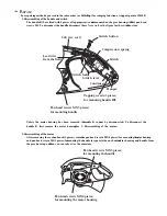
Note) Keep the document
guide upper unit in the rib
of operation panel unit
like a picture.

Note) Keep the operation
panel PWB to under the
rib like a picture.

Rib

6

LCD PWB

LCD PWB

Rib

Rib

LCD CABLE

Note) The LCD PWB should 
        be securely locked by the 
        click of the panel case.

6

Rib

6

Note) Keep the operation
panel PWB to under the
rib like a picture.

1

Note) Keep the document
guide upper unit to under
the rib like a picture.

Rib

2

3

Summary of Contents for FO-780A

Page 1: ... control PWB 5 2 3 Circuit description of TEL LIU PWB 5 8 4 Circuit description of power supply PWB 5 11 5 Circuit description of CIS unit 5 11 CHAPTER 6 CIRCUIT SCHEMATICS AND PARTS LAYOUT 1 Control PWB circuit 6 1 2 TEL LIU PWB circuit 6 9 3 Power supply PWB circuit 6 11 4 Operation panel PWB circuit 6 13 CHAPTER 7 OPERATION FLOWCHART 1 Protocol 7 1 2 Power on sequence 7 2 CHAPTER 8 OTHERS 1 Ser...

Page 2: ... ohjeiden mukaisesti French ATTENTION Il y a danger d explosion s il y a remplacement incorrect de la batterie Remplacer uniquement avec une batterie du même type ou d un type recommandé par le constructeur Mettre au rébut les batteries usagées conformément aux instructions du fabricant Swedish VARNING Explosionsfare vid felaktigt batteribyte Använd samma batterityp eller en ekvivalent typ som rek...

Page 3: ...hod Sheet feeder CIS Contact Image Sensor Effective recording width 204 max Input document size Automatic feeding Width 148 to 210 mm Length 140 to 297 mm Manual feeding Width 148 to 210 mm Length 140 to 600 mm Effective scanning width 210 mm max Contrast control Automatic Dark selectable Copy function Standard Telephone function Standard cannot be used for incoming outgoing if power fails Power r...

Page 4: ...me storing procedures 10 HOLD SEARCH key Press this key to search for an automatic dialing number or during a phone conversation press this key to put the other party on hold 11 SPEAKER key Press this key to hear the line and fax tones through the speaker before sending a document or dialing a voice number Note This is not a speakerphone You must pick up the handset to talk with the other party 12...

Page 5: ...rrier sheet for smaller documents Normal size ADF 10 sheets 2 4 10 3 3 4 10 3 inch 0 06 0 09 mm Thickness Weight 0 15 10 3 lbs inch2 52 80g m2 14 20lbs Special size Thickness 2 4 10 3 7 9 10 3 inch 0 06 0 20 mm 0 15 10 3 0 20 10 3 lbs inch2 52 157g m2 Weight Readable width 3 Document Types Normal paper Documents handwritten in pencil No 2 lead or softer fountain pen ball point pen or felt tipped p...

Page 6: ...urge protectors can be purchased at most telephone specialty stores If the machine is moved from a cold to a warm place If the machine is moved from a cold to a warm place it is possible that the reading glass may fog up preventing proper scanning of documents for transmission To remove the fog turn on the power and wait approxi mately 2 hours before using the machine TELEPHONE JACK A standard tel...

Page 7: ...ders FTurn the cartridge over grasp the handle and insert the cartridge into the print compartment Slot Protrusion Large gear 8Insert the large gear into the large holder on the imaging film cartridge make sure it clicks into place and then insert the small gear on the other end of the spool into its holder GRotate the large gear toward you until the film is taut HClose the print compartment cover...

Page 8: ...he telephone line cord into the TEL LINE socket Do not Insert into the TEL SET socket 5Attach the original document support Note The original document support has a top side and a bottom side If you cannot insert the tabs on the support into the holes turn the support over Make sure the handset cord goes into the socket marked with a handset symbol on the side of the machine Use the handset to mak...

Page 9: ...rmal contrast Depending on the type of paper you have loaded you may find that you obtain better print quality by changing the setting to LIGHT Press these keys 5 Clearing a jammed document If the original document doesn t feed properly during transmission or copying or DOCUMENT JAMMED appears in the display first try pressing the START MEMORY key If it doesn t feed out remove it as follows Import...

Page 10: ...side of the machine forward to open the print compartment cover 4Close the print compartment cover press down on both sides to make sure it clicks into place and then close the operation panel 3Gently pull the jammed paper out of the machine making sure no torn pieces of paper remain in the print compartment or rollers 5Reinsert the paper in the paper tray and push the paper release plate back dow...

Page 11: ...r 3 Press RECEIVING DOCUMENTS Press FAX mode The fax automatically answers on four rings and receives the incoming document TEL mode TEL FAX mode The fax machine automatically answers on two rings and receives faxes Voice calls including manually dialed fax transmissions are signalled by a special ringing sound A M mode Select this mode when an answering machine is connected to the fax and the ans...

Page 12: ...NP standard ink film HC Heading Requirements Measuring method Material Polyethylene terephthalate Heading Requirements Measuring method Grade HR Mixer P 5 Heading Requirements Measuring method Grade ML Sumi Heading Requirements Measuring method Grade 507W 2 Details of compositions 2 1 Base film 2 2 Heat resistant layer 2 3 Matt layer 2 4 Hot melt ink layer 1 2 3 4 1 2 3 4 Heat Resistant Layer Base...

Page 13: ...V 24 7V 2 IC protectors replacement ICPs IC Protectors are installed to protect the motor driver circuit ICPs protect various ICs and electronic circuits from an overcurrent con dition The location of ICPs are shown below 1 MG 2 MG 3 24V 4 24V 5 24V 6 DG 7 5V 8 DG 9 PSAVE Connector No CNPW Pin No 2 1 TEL LIU PWB POWER SUPPLY PWB CONTROL PWB CNLIUA CNLIUA CN1 CNPW CNTH CNPN CNCIS CNSP CNMT CNCSW CN...

Page 14: ...ed and RAM is matched Result list is output 3 3 AGING MODE 10 sheets of check patterns are output every 5 minutes per sheet 4 4 PANEL KEY TEST Panel keys are tested Result list is output 5 5 CHECK PATTERN Check pattern is output 6 6 SIGNAL SEND MODE Various signals of FAX communication are output 7 7 MEMORY CLEAR Back up memory is cleared and is set at delivery 8 8 SHADING MODE Shading compensatio...

Page 15: ...ssed on one line 2 Full black Approx 30 mm 3 6 Signal send mode This mode is used to send various signals to the circuit during FAX com munication Every push of START key sends a signal in the following sequence Moreover the signal sound is also output to the speaker when the line monitor of the soft switch is on 1 No signal CML signal turned on 2 9600bps 3 7200bps 4 4800bps 5 2400bps 6 300bps FLA...

Page 16: ... 4 How to make soft switch setting To enter the soft switch mode make the following key entries in se quence 2 4 Press FUNCTION 9 8 7 START START Press FUNCTION key Press key Press key Bit1 8 are set Soft SW A2 SW M2 are set S F T SW A1 1 0 0 0 0 0 0 0 S F T SW A1 1 0 0 0 0 0 0 0 S F T SW A1 1 0 0 0 0 0 0 0 S F T SW A1 1 0 0 0 0 0 0 0 S F T SW A2 0 0 0 0 0 0 0 0 S F T SW M2 0 0 0 0 0 0 0 0 Press k...

Page 17: ...rror 0 sending mode reception 8 CNG transmission No Yes 0 CED tone signal interval 1000ms 750ms 500ms 75ms 1 No 1 1 1 0 0 0 2 No 2 1 0 1 0 0 3 MR coding No Yes 0 4 Reserved 0 5 Reserved 0 6 Reserved 0 7 Reserved 0 8 Reserved 0 1 Signal transmission level Binary input 0 2 No 16 8 4 2 1 1 3 1 2 3 4 5 1 4 0 1 1 1 1 1 5 1 6 Protocol monitor error print Printed at com err Not printed 0 7 Protocol monit...

Page 18: ... Reserved 0 5 Waiting time after dialing 90 sec 45 sec 0 6 Reserved 0 7 Reserved 0 8 Reserved 0 1 Reserved 0 2 Reserved 0 3 Reserved 0 4 Reserved 0 5 Reserved 0 6 Reserved 0 7 Reserved 0 8 Reserved 0 1 Auto Dial Mode Delay timer of before line 3 sec 0 sec 1 connect 2 Auto Dial Mode Delay timer of after line 3 6 sec 3 sec 0 connect 3 Dial mode Tone Pulse 1 OPTION 4 Pulse Tone change function by key...

Page 19: ...ved 0 8 Reserved 0 1 Reserved 0 2 Reserved 0 3 Reserved 0 4 Distinctive ringing detection Yes No 0 OPTION 5 Caller ID function Yes No 0 OPTION CI off detection timer Distinctive ring 1200ms 1000ms 700ms 350ms 6 setting off only No 6 0 1 0 1 0 7 No 7 0 0 1 1 1 8 Caller ID detect during CI off All times Only first 1 1 Tel Fax Automatic switching mode Tel Fax auto switch Switch to Fax 1 Pseudo ringin...

Page 20: ...o 2 0 0 1 1 0 3 No 3 0 1 0 1 1 Number of CNG STAND BY mode 1pulse 2pulses 3pulses 4pulses 4 No 4 0 0 1 1 0 5 No 5 0 1 0 1 1 6 Reserved 0 7 Reserved 0 8 Reserved 0 1 Quiet detect time Binary input 0 OPTION 2 No 8 4 2 1 1 3 1 2 3 4 0 4 0 1 0 0 0 5 Quiet detect start timing Binary input 0 6 No 8 4 2 1 1 7 5 6 7 8 0 8 0 1 0 1 1 1 Reserved 0 2 Reserved 0 3 Reserved 0 4 Reserved 0 5 Reserved 0 6 Reserve...

Page 21: ... 2 No 2 0 1 0 1 1 3 Fax switching when A M full Yes No 0 OPTION 4 Reserved 0 5 Reserved 0 6 Reserved 0 7 Reserved 0 8 Reserved 0 1 Reserved 0 2 Reserved 0 3 Reserved 0 4 Reserved 0 5 Reserved 0 6 Reserved 0 7 Reserved 0 8 Reserved 0 1 Reserved 0 2 Reserved 0 3 Reserved 0 4 Reserved 0 5 Reserved 0 6 Reserved 0 7 Reserved 0 8 Reserved 0 1 Reserved 0 2 Reserved 0 3 Reserved 0 4 Reserved 0 5 Reserved ...

Page 22: ... change Change allowed 0 4 Reserved 0 5 Reserved 0 6 Reserved 0 Ringer volume Off Low Middle High OPTION 7 No 7 0 0 1 1 1 8 No 8 0 1 0 1 0 Speaker volume 3 stages Low Low Middle High OPTION 1 No 1 0 0 1 1 1 2 No 2 0 1 0 1 0 3 Polling key Yes No 0 OPTION 4 Reserved 0 5 Reserved 0 6 Reserved 0 7 Reserved 0 8 Reserved 0 1 Automatic cover sheet Yes No 0 OPTION Communication results printout E T M Send...

Page 23: ...R LEGAL A4 1 No 1 0 0 1 1 2 No 2 0 1 0 0 3 Automatic reduce of receive Auto 100 1 OPTION 4 Print contrast Light Normal 0 OPTION 5 Reception reduction ratio in case of memory full 100 93 0 OPTION 6 Reserved 0 7 Reserved 0 8 Reserved 0 1 Reserved 0 2 Reserved 0 3 Reserved 0 4 Reserved 0 5 Reserved 0 6 Reserved 0 7 Reserved 0 8 Reserved 0 1 Reserved 0 2 Reserved 0 3 Reserved 0 4 Reserved 0 5 Power sa...

Page 24: ... TRANSMISSION is a switch to set the function to print the content of HEADER PRINT described in the passcode list at the front end of receiver s original when original is sent to the remote machine If this switch is set to NO the HEADER PRINT is not output at the receiving machine SW A2 No 6 H2 mode Used to determine reception of H2 mode 15 sec transmission mode When set to OFF H2 mode reception i...

Page 25: ...n telephone numbers of direct dial con nection Selection of 4 sec or 2 sec pause is available SW B2 No 2 No 4 Reserved Set to 0 SW B2 No 5 Waiting time after dialing This is time waiting for the opponent s signals after dialing For the Switzerland version the time is fixed to 90 seconds regardless of this switch setting SW B2 No 6 No 8 Reserved Set to 0 SW B3 No 1 No 8 Reserved Set to 0 SW B4 No 1...

Page 26: ...g mode SW E1 No 4 Number of CNG signal detection at the phone fax automatic switching mode Used for detection of CNG in one tone or two tones in the TEL FAX automatic switching mode SW E1 No 5 CNG detect time at TEL FAX mode The switch which sets the time from the start of CNG detection to the end of detection SW E1 No 6 Reserved Set to 0 SW E1 No 7 Post answer tone transmit in TEL FAX mode When s...

Page 27: ...ake a choice of whether the registered sender s phone number can be changed or not If the switch is set to 1 new registration of the sender s phone number is disabled to prevent accidental wrong input SW J1 No 4 No 6 Reserved Set to 0 SW J1 No 7 No 8 Ringer volume Used to adjust ringing volume SW J2 No 1 No 2 Speaker volume 3 stages Used to adjust sound volume from a speaker SW J2 No 3 Polling key...

Page 28: ...the recording paper SW L2 No 3 Automatic reduce of receive If set to 1 it is reduced automatically when receiving SW L2 No 4 Print contrast 0 Normal 1 Light SW L2 No 5 Reception reduction ratio in case of memory full This model is designed so that the print is started according to the setting of SW L2 No 3 when reception of one page is completed However if the memory is filled with data before com...

Page 29: ... format and check the related matters TO ATT Ref No CC ATT Date FM Dept Sign 2 17 Please complete this report before calling the TAC hotline if problem still occurs Facsimile communication problem Ref No Date From Mr Fax Tel No Our customer Name Tel No Address Fax No Contact person Model name Other party Name Tel No Address Fax No Contact person Model name Problem mode Line Domestic international ...

Page 30: ...rred just after fallback 13 Error occurred after a response to retransmission end command was received G3 Reception Code Final received signal Error Condition Receiver side 0 Incomplete signal frame Cannot recognize bit stream after flag 1 NSS DCS Cannot recognize CFR or FTT signal Disconnects line during transmission line error 2 NSC DTC Cannot recognize NSS signal FIF code etc 3 EOP Cannot recog...

Page 31: ...he paper feed roller to assure smooth feed ing of the document 2 Document separation method Separation rubber plate Fig 3 3 3 Documents applicable for automatic feed NOTE Double side coated documents and documents on facsimile re cording paper should be inserted manually The document feed quantity may be changed according to the document thickness Documents corresponding to a paper weight heavier ...

Page 32: ...g elements in traverse line and the resolution power is 8 dots mm The maximum speed is 10 ms line 2 Structure of recording mechanism Recording is achieved by applying a suitable pressure to the thermal head through the imaging film of the recording paper feed roller and the recording paper The main scanning is electronically done and the sub scanning is me chanically done by sending the recording ...

Page 33: ...ts refer to the Parts List The numbers in the illustration the parts list and the flowchart in a same section are common to each other To assure reliability of the product the disassembly and the assembly procedures should be performed carefully and deliberately Bottom plate 1 Parts list Fig 1 Fig 1 4 Head earth cable 1 5 Screw 3 6 1 6 Shield sheet 1 7 Bottom plate 1 No Part name Q ty No Part name...

Page 34: ... Part name Q ty 1 Mechanism unit 1 2 Connector 3 3 Cable 6 4 Control PWB unit 1 5 TEL Liu PWB unit 1 6 Power supply PWB unit 1 3 4 4 6 6 7 8 8 5 11 11 12 12 10 10 9 9 1 9 2 2 3 3 3 3 4 Control PWB Top view 3 AC cord earth cable AC cord earth cable 2 3 4 5 6 1 7 6 Note Keep the power supply PWB unit to under the rib like a picture Rib Position of AC cord 8 The number direction keep on top side 3 2 ...

Page 35: ... Part name Q ty No Part name Q ty 1 Mechanism unit 1 2 Sheet A 1 3 P IN sensor lever B 1 4 PE sensor lever B 1 5 PE sensor lever spring B 1 6 Screw 3 10 1 7 BT gear ass y 1 12 13 13 14 14 1 1 2 2 3 3 4 4 5 5 6 7 7 1 13 Fix size 271 8 0 4mm An attachment rib is attached in cccordance with hole right and left 10 10 10 11 11 6 8 8 8 9 9 9 13 Rib 12 Applying position for SHEET A Clean apply area by Al...

Page 36: ...2 3 3 4 4 4 5 5 1 7 7 7 7 9 8 6 6 12 11 13 12 14 13 15 14 11 10 15 17 16 16 16 10 9 9 16 15 15 18 20 19 19 19 18 18 21 21 22 22 22 23 23 23 18 17 26 25 25 24 24 CAUTION Do not apply FLOIL to this gear Please wipe off when FLOIL sticks to this gear Grease Grease Nail be doing lock To be the switch linked by hooks Boss Boss Nail Nail GEAR attachment boss NOTE Apply certainly to a part of a nail at t...

Page 37: ...ation panel unit and CIS unit 5 2 2 1 3 3 4 4 4 5 5 7 7 8 8 9 9 9 6 6 11 13 12 12 14 13 14 10 11 10 1 1 2 3 1 4 5 6 Operation panel unit disassembly Close insignificantly the operation panel unit from the FULL OPEN position 2 Shift the operation panel unit to the left side and remove the left side fulcrum 3 Shift the operation panel unit to the right side and remove the right side fulcrum 4 Sub fr...

Page 38: ...per cabinet 1 6 2 2 1 1 3 3 4 4 4 4 4 4 6 5 5 7 7 8 8 9 9 6 12 12 11 11 10 10 2 3 Note Keep the document guide upper unit in the rib of operation panel unit like a picture Note Keep the operation panel PWB to under the rib like a picture Rib 6 LCD PWB LCD PWB Rib Rib LCD CABLE Note The LCD PWB should be securely locked by the click of the panel case 6 Rib 6 Note Keep the operation panel PWB to und...

Page 39: ...rts list Fig 7 No Part name Q ty No Part name Q ty 1 Back roller gear 1 2 Transfer bearing 1 3 Back roller 1 4 Pinch roller spring 2 5 Pinch roller 2 6 Pinch roller shaft 1 Document guide upper 7 Confirm hook is locked Confirm Thing which does not run aground 2 2 1 1 3 3 4 4 4 4 4 5 5 5 5 7 7 7 8 8 8 9 9 9 6 6 6 12 12 12 12 12 11 11 10 10 1 1 2 12 ...

Page 40: ...ame unit 1 4 RP hopper unit 1 5 Sub frame ass y 1 6 Screw 3 10 1 7 Tension gear 1 8 Tension spring 1 9 PO guide ass y 1 Fig 8 Sub frame top cover unit RP hopper unit 8 3 10 Parts list Fig 8 No Part name Q ty No Part name Q ty No Part name Q ty 2 2 2 1 3 3 4 4 4 5 5 5 7 8 9 9 6 7 8 6 12 13 13 13 14 14 15 26 27 15 15 11 11 17 17 18 19 9 12 11 10 10 10 16 16 22 23 24 25 21 20 18 18 19 20 19 22 23 24 ...

Page 41: ... 1 4 Hopper spring 1 5 Hopper guide right 1 6 Hopper guide left 1 7 TC sheet 1 8 Top cover 1 R L GAP 0 GAP 0 HOPPER GUIDE L HOPPER GUIDE R 30 Fix position boss Rib Rib Cross section Upper figure Do not run aground in the rib 0mm 0mm 0mm 0mm Applying standard Applying standard Note Hopper guides move smoothly Operation load is 450 g range from 80 g Confirm of HOPPER GUIDE position 2 2 10 1 1 3 3 4 ...

Page 42: ...d spring E 2 14 Head spring B 2 15 Head spring F 1 16 Head cushion 2 17 Head frame 1 18 Head cable 1 19 Screw 3 6 1 20 Head guide right 1 21 Screw 3 6 1 22 Head guide left 1 23 Thermal head 1 Tightening torque 6 0 0 5kg cm Put the earth cable in parallel to the head frame Install the spring on the ditch of the rib The head and head earth cable pass to the core 2 times 2 2 1 3 3 4 4 4 4 5 5 7 7 7 8...

Page 43: ...The Head cable and Head earth cable pass to the core 2 times The panel cable pass to the core 2 times panel cable Operation panel PWB Panel cable Operation panel unit Operation panel unit Document guide upper unit Panel cable Document guide upper unit Control PWB Head cable Head earth cable Panel cable Motor cable Cam switch cable Rib Rib Rib Rib Speaker cable Lower cabinet Drive unit 5 CIS cable ...

Page 44: ...FAX ENGINE FC200 M HANDSET SPEAKER 5V 24V OPERATION PANEL TEL LIU PWB UNIT DRIVER THERMAL HEAD PM CONTACT IMAGE SENSOR DOCUMENT SENSOR POWER SUPPLY PWB UNIT DRAM 4Mbit REGULATOR SELECT SPEAKER AMPLIFIER AMPLIFIER AMPLIFIER SURGE PROTECT FILTER CML TRANSFORMER CI VBT STABILIZER RECTIFIER TRANSFORMER RECTIFIER DIODE TRANS SURGE ABSORBER FILTER LINE EXT TEL P IN SENSOR RESET IC AMPLIFIER BZ CLOCK 19 ...

Page 45: ... LCD UNIT CNLCD OPERATION PANEL PWB NUIT 14 CNPN 16 7 15 CNCSW CNMT CNTH CNCIS CNPN CNSP SPEAKER CNLIUA CNPW 14 9 CONTROL PWB UNIT TEL LIU PWB UNIT POWER SUPPLY PWB UNIT CNLIUA CN1 EXTERNAL LINE TEL LINE MJ1 2 MJTEL AC CORD TX RX MOTOR 2 HANDSET FG FG FG ARG 6 CNLIUB CNLIUB ...

Page 46: ... KEN2A KEN1A DG DG 5V ORGSNS FRSNS E SEN4 SEN0 SEN1 SEN2 SEN3 KEN4A KEN3A KEN2A KEN1A DG DG 5V ORGSNS FRSNS E SEN4 SEN0 SEN1 SEN2 SEN3 CNPN CNPN CNCIS 1 2 3 4 5 6 7 8 9 10 11 12 13 14 1 2 3 4 5 6 7 8 9 10 11 12 13 14 TEL LIU PWB TELOUT TELIN TELMUTE CI CIDIN1 CIDIN2 HS PE PIN RHS RXIN TXOUT CML 5V DG 24V TELOUT TELIN TELMUTE CI CIDIN1 CIDIN2 HS PE PIN RHS RXIN TXOUT CML 5V DG 24V CNLIUA CNLIUA CNM...

Page 47: ...it buffer of the RAM The data is then con verted from parallel to serial form by the modem where the serial data is modulated and sent onto the line Receive operation There are two ways of starting reception manual and automatic Depression of the START key in the off hook mode in the case of manual receive mode or CI signal detection by the LIU in the auto matic receive mode First the FC200M contr...

Page 48: ...L EXTERNAL DECODE DMA CONTROLLER OPERATOR PANEL IF 32 KEYS 8 LEDS LCD MODULE MOTOR POWER CONTROL RINGER SYNC SERIF 1 THERMAL PRINTER IF 5 ms LINE TIME A4 B4 LINES TPH ADC 4 STROBE TPH LATCHLESS TPH EXTEMAL DMA I F T 4 T 6 CODEC MH MR MMR HARDWARE ALTERNATE COMPRESSION DECOMPRESSION BI LEVEL RESOLUTION CONVERSION PROGRAMMABLE REDUCTION EXPANSION 2 6kBYTE VIDEO RAM SCANNER CONTROL VIDEO PROCESSING 8...

Page 49: ...battery power but the output drive is powered by DRAM battery power Scanner Interface START 101 O 2XS Scanner shift gate control CLK1 100 O 2XS Scanner clock CLK1n 99 O 2XS Scanner clock inverted CLK2 98 O 2XS Scanner reset gate control or clock for CIS scanner FCS1n VIDCTL0 96 O 2XT Flash memory chip select or Video Control signal FCS2n VIDCTL1 97 O 2XT Flash memory chip select or Video Control s...

Page 50: ...O H 2XC Hysteresis In GPIO 13 or I O chip select 3 GPIO 14 CS 4 n 78 I O H 2XC Hysteresis In GPIO 14 or I O chip select 4 GPIO 15 CS 5 n 77 I O H 2XC Hysteresis In GPIO 15 or I O chip select 5 GPIO 16 IRQ 8 76 I O H 1XC Hysteresis In GPIO 16 or external interrupt 8 GPIO 17 IRQ 5 n 75 I O H 1XC Hysteresis In GPIO 17 or external interrupt 5 GPIO 18 IRQ 9 n 74 I O H 1XC Hysteresis In GPIO 18 or exter...

Page 51: ...RT CLK2 CLK1 CLK1N VIDCTL 1 0 XIN XOUT MIRON MCSN SYSCLK D 7 0 RDN A 4 0 WRN MONOFAX FACSIMILE MODEM ANALOG SWITCH LINE INTERFACE SPEAKER MICROPHONE CIRCUIT TELEPHONE LINE RXA TXA SPKR MIC RIN SPKRLO SPKRHI SPKR RIN TXA2 TXA1 TXOUT RXIN XIA GPIO DRAM OPTION SCANNER VIDEO PREPROCESSING SYNC PORTS 2 SSIF VIN VREF VREF SSCLK 2 1 SSTXD 2 1 SSRXD 2 1 SSSTAT 2 1 SYNC ASYNC SERIAL PORT SASCLK SASTXD SASR...

Page 52: ... pin plastic quad flat pack PQFP or a 64 pin quad in line package QUIP General purpose input output GPIO pins are available for host as signment in the 100 pin PQFP The modem s small size single voltage supply and low power con sumption allow the design of compact system enclosures for use in both office and home environments MONOFAX is a registered trademark of Rockwell International FEATURES Gro...

Page 53: ...49 AOUT R 50 0VD1 GND 51 NC 52 IRQ OC 53 WRITE R W IA 54 CS IA 55 READ φ2 IA 56 RS4 IA 57 RS3 IA 58 RS2 IA 59 RS1 IA Pin No Signal Name I O Type 60 RS0 IA 61 GP13 IA OB 62 NC 63 GP11 IA OB 64 RTS IA 65 EN85 R 66 0VD2 GND 67 PORI ID 68 XTLI R 69 XTLO R 70 XCLK OD 71 YCLK OD 72 5VD1 PWR 73 DCLK1 R 74 SYNCIN2 R 75 GP16 IA OB 76 GP17 IA OB 77 0VD2 GND 78 CTS OA 79 TXD IA 80 0VD2 GND 81 0VD2 GND 82 DCL...

Page 54: ...N HOOK OFF HOOK HOOK SW RHS RHS TEL MUTE TEL MUTE SPMUTE L H DG VOL B VOL A BZCONT DPON CML FC200M TXOUT VOL A VOL B TXMUTE DPMUTE RCVOL2 RCVOL RXIN E RLY RCVOL DG SPEAKER L H BZOUT TXCONT GAINC SIGMUTE Fig 5 2 Circuit description The TEL LIU PWB is composed of the following 10 blocks 1 Surge protection circuit 2 Noise filter 3 Dial pulse generation circuit 4 CML relay 5 Matching transformer 6 Hyb...

Page 55: ...N and the detection level is LOW When there is no recording paper the photo transistor in the light receiving side is OFF and the detection level is HIGH 9 CI detection circuit The CI detection circuit detects the CI signals A CI signal which is provided to the photo coupler PC6 through the C3 0 56 µF R3 22 K and ZD2 when the ring signal is inputted from the telephone line 10 Power supply and bias...

Page 56: ...m line or modem TEL OUT Transfer signal to line TXOUT Transmission DTMF analog signal output from modem RXIN Reception DTMF others analog signal input into modem Other signals NO Signal Name CNLIUA 8 RHS 9 RXIN 10 TXOUT 11 CML 12 5V 13 DG 14 24VA NO Signal Name CNLIUB 1 EXTSIG 2 RLYCNT 3 SIGMUTE TXMUTE NO Signal Name CNLIUB 4 DPON 5 DPMUTE 6 RCVOL H L H L CML CI DETECT LINE EXT HI GAIN TXOUT TXMUT...

Page 57: ... capacitor C2 to supply DC voltage to switching circuit section Power thermistor TH1 suppresses inrush current at power switch on 2 3 Switching circuit This circuit employs the self excited ringing choke convertor RCC sys tem In this system the DC voltage supplied from the rectifying smooth ing section is converted to be the high frequency pulses by ON OFF repetition of MOS FET Q1 Energy is charge...

Page 58: ...14 A13 A12 A11 A10 A9 A8 A7 A6 A5 A4 A3 A2 A1 A0 32 C162 0 1 5V RA5 270x4 90 GPIO4 100 CLK1 30 PDAT 24 A3 57 CS0 GPIO3 GPIO2 GPIO1 GPIO0 R227 CNPW 9 PSAVE CNLIUA 11 100Px5 CNLIUA 8 RHS CNLIUA 5 HS CI TELMUTE BYPASS R183 470 R161 470 R160 30K STRB3 CNTH 4 STRB2 CNTH 3 PCLK DATA CNTH 14 CNTH 15 CNTH 13 LATCH R143 470 R142 150 RA12 100x4 R163 100 R190 100 R191 100 STRB4 CISCLK STRB1 R189 10K C172 68P...

Page 59: ...R A16 21 A15 20 A14 29 19 A13 28 18 A12 17 A11 25 15 A10 23 14 A9 26 13 A8 27 A7 A6 31 A5 32 A4 1 A3 A2 10 A1 11 16 A0 12 5V C107 0 1 D7 D6 D5 D4 D3 D2 D1 D0 IC4 27C020 2 A16 D7 3 A15 D6 A14 D5 A13 D4 4 A12 D3 A11 D2 A10 D1 A9 D0 A8 5 A7 6 A6 VCC 7 A5 PGM 8 A4 VPP 9 A3 A2 A1 GND A0 A17 30 A17 DG DG C234 N M CE OE 22 24 ROMCS 1 3H C216 0 1 R106 0 DG 20 CE1 CE2 1 3H 2 2I CS1 1 21 A14 3 20 A13 28 19 ...

Page 60: ... 27 29 31 32 C3 47 25 R155 3 5V R137 0 MAG N C 33 SIGRX 5 4 3 2 1 100 63 38 39 40 85 25 83 26 74 84 86 90 68 GP07 GP06 GP05 GP04 GP03 GP02 GP11 TXLOSS2 TXLOSS1 EYECLK ECLKIN1 EYESYNC SYNCIN1 SYNCIN2 EYECLKX EYEX EYEY XTLI DPMUTE RCVOL VREFCONT 5 5F 6 1I 5 1A 6 2E R141 1000P MAG X2 24 00014MHz C113 15P R126 120 C123 18P R125 200 69 XTLO IC6 R96DFXL CID N C N C N C DG 6 3A VOLB LEDON D 7 0 RD WR 1 6...

Page 61: ...SNS 5V R221 220 1 3 2 4 PI1 SG206 DG HOLBAT 1 BT R134 5 6K CNPW 7 5V HOLBAT 2 HOLBAT 3 DG BAT1 CR2032 DG D102 RB705D 5V VBT VBT 5V CNPW 6 DG CNLIUA 12 5V CNLIUA 13 CNPN 5 DG CNPN 6 CNCSW 2 DG C201 0 1 C8 47 25 DG CNPW 3 24V CNPW 1 CNPW 2 C200 0 1 C6 22 50 R222 24V MG N M 24VA DG C7 100 50 DG CNPW 8 CNLIUA 14 24V CNPW 4 24V CNPW 5 R223 N M C222 C221 C219 R102 270 C220 N M N M DG DG DG DG DG R105 27...

Page 62: ...82 0 Q1 Q110 E B C 3 1D VREFCONT 5 5H LEDON COM 9 1 1B 1C 16 2 2B 2C 15 3 3B 3C 14 4 4B 4C 13 5 5B 5C 12 6 6B 6C 11 7 7B 7C 10 8 E TPA TPB 1 1E TPA 1 1E TPB 1 1E 1 1E 3 1D LEDON IC5 ULN2003A CNMT 5 CNMT 6 CNMT 4 CNMT 3 CNMT 2 CNMT 1 LEDON 5 2B 24V D2 1N4748A FU100 ICPS07 MG MG VTH CNTH 1 CNTH 2 CNTH 16 MG CNTH 7 CNTH 8 CNTH 9 MG 5V CNTH 10 THADI 1 1F THI CNTH 5 MG MG C174 1 R164 20K C5 10 50 R165 ...

Page 63: ...CNLIUA 9 R213 3 9K R195 118K R214 0 EXSIG CNLIUB 1 C194 0 R198 47K 14 13 12 24VA R196 1 5K C182 1 R177 47K R201 10K TELIN CNLIUA 2 C180 1000P C184 0 1 11 4 VREF 5V C160 0 1 R181 33K IC12 2902 R180 33K C161 1 1 15 2 10 IC11 4053 1 R174 1K C158 4700P R166 100K R168 1K C159 0 01 R173 20K R192 1K R175 20K R170 3K C2 1 50 5 IC10 NJM2113 8 7 1 3 2 4 6 R167 30K 5V R171 100K R172 220K C157 220P SP CNSP 1 ...

Page 64: ...FO 780A Control PWB parts layout Top side 6 7 ...

Page 65: ...FO 780A Control PWB parts layout Bottom side 6 8 ...

Page 66: ...29 R147 470 R142 470 C115 2200P R149 30K IC102 2904 R127 20K C131 0 1 TXOUT VREF A CNLIUA 10 PC4 PC5 R117 R105 N M D S G R109 15 ZD4 MTZJ6R8B R107 15 C1 4 7 50 R119 10K R108 13K PC2 TLP521 ZD5 MTZJ30B PC3 TLP627 REC1 S1ZB60 R1 4 7mH ZD6 HZ2A1 ZD7 HZ2A1 C108 N M T1 I2142 C103 0 047 C2 1 0 C4 0 33 R103 300 R102 43K C3 0 56 ZD3 0 D3 1SS131 PC6 TLP521 ZD2 MTZJ20B 9 8 10 CML AR1 RA 501P AR2 RA 501P ARG...

Page 67: ...1 R132 CNLIUB 5 DPMUTE Q109 RNC1402 DG PC2 TLP521 R133 470 CNLIUB 4 DPON Q108 RNC1402 DG PC3 TLP627 R131 470 CNLIUA 4 CI 5V R140 100K C112 0 1 DG DG PC6 TLP521 CNLIUA 5 HS R129 C109 DG DG PC4 5V N M C11 22 50 Q102 RNC1402 DG R168 10 CNLIUA 6 CNLIUA 7 P E P IN R126 130 P IN SG 206 PE SG 206 DG DG CNLIUB 2 RLYCNT 1 12 S RLY D2 Q101 DG R165 R164 N M CNLIUB 3 SIGMUTE DG Q107 RNC1402 R162 R163 DG A N M...

Page 68: ...FO 780A 6 11 TEL LIU PWB parts layout Top side ...

Page 69: ...FO 780A TEL LIU PWB parts layout Bottom side 6 12 ...

Page 70: ...W IC1 NJM2391FO5 C8 330 35 C11 0 1 C10 2200 16 R11 39 1 8W ZD3 RD20ESAB PC1 PC 123YS R12 330K 1 8W Q5 2SC1710 Q6 2SC1710 R20 4 7K 1 8W C9 0 47 R19 47K 1 8W R13 270 1 8W R18 3 9K 1 8W PC2 PC 123YS R14 N M Q4 2SC1710 ZD5 RD6 2ESAB VR1 500 R17 2 4K 1 8W R16 6 8K 1 8W D2 ERA15 06 D3 ERA15 06 D4 ERA15 06 C15 0 1 TH1 8 2 F2 1 6A 250V C3 470P Q1 FS5KM 18 ZD1 RD27ESAB Q3 2SC1740S R9 470 1 8W R10 0 33 1W R...

Page 71: ...FO 780A Power supply PWB parts layout 6 14 ...

Page 72: ...LCD 2 CNLCD 1 C2 22 50 C1 2200P CNLCD 11 LD4 CNPN 4 CNLCD GND 1 2 3 4 5 6 7 8 9 10 11 12 13 14 5V VO RS R W E N C N C N C N C LD4 LD5 LD6 LD7 CNPN KEN4 KEN3 KEN2 KEN1 5V DG DG ORGSNS FRSNS E SEN4 SEN0 DOWN RESOLUTION PLAY DELETE STOP START 5 9 3 6 HOLD SPEAKER SPEED REDAIAL 05 07 01 03 06 08 02 04 7 1 4 D1 1SS270 D2 1SS270 D4 1SS270 D3 1SS270 CNLCD 12 LD5 CNLCD 13 LD6 CNLCD 14 LD7 15 N C 5V VCC GN...

Page 73: ... RTC EOP MCF DCN IMAGE SIGNAL Document ejected Recording papor ejected Receive side G3 communication CED Transmitter side Document inserted into document sensor during standby To recording position DCS Cut line printed IMAGE SIGNAL Cut line printed IMAGE SIGNAL IMAGE SIGNAL Next page insert command 1st page Document inserted to the reading position DCS ...

Page 74: ...EM initialized STOP key WAIT A MOMENT display START NO YES STAND BY 3 sec NO MEMORY CLEAR display NO YES STAND BY 3 sec NO NO START key COPY key STOP key NO Memory clear STAND BY 2 1 MEMORY CLEARED display Memory clear PROCESS CHECK MODE MEMORY CLEARED display YES ...

Page 75: ...ITCH RELAY CABLE 1 AK 6 C C N W 4 7 6 3 S C 0 1 MOTOR RELAY CABLE 1 AP 7 Q C N W 4 9 6 9 S C Z Z PAPER SENSOR RELAY CABLE 1 BF 8 V R S T S 2 A D 2 2 1 J RESISTOR 1 10W 220Ω 5 R221 1 AA 9 V H P S G 2 0 6 S 1 PHOTO TRANSISTOR PI1 1 AG 10 Q S W M 2 2 5 9 X H Z Z COVER SWITCH SW1 1 AF 11 Q C N C M 2 5 7 5 S C 1 D CONNECTOR 14PIN CNLIUA 1 AC 12 V R D H T 2 E Y 1 0 1 J RESISTOR 1 4W 100Ω 5 R20 1 AA 13 V...

Page 76: ...on with mechanical unit Recording paper sensor ON OFF operation OFF Photo interrupter is interrupted PWB sensor check Recording paper sensor ON OFF operation OFF POWER SUPPLY PWB CHECK TEL LIU PWB CHECK CONTROL PWB RELAY CABLE DON T SEPARATE UNIT NOTE PAPER SNSOR RELAY CABLE QCNW 4969SCZZ TO CHECK PWB TO EXTENSION PWB 5V J13 DG J5 P E TP2 P IN TP3 RBNSNS DRSNS TEL LIU TEL LIU TEL LIU TEL LIU CONTR...

Page 77: ...ck basis is applied to remember the shading wave form Be sure to perform this operation when replacing the battery or replacing the control PWB Execute in the shading mode of DIAG mode UX 300 SERIES SHADING WAVE MEMORY STANDARD PAPER PSHEZ3354SCZZ ...

Page 78: ...3Y VCC 6A 6Y 5A 5Y 4A 8 4Y 7 GND Signal A0 A14 CS1 CS2 WE OE I O1 I O8 VDD VSS Address input Chip enable Write enable Write enable Data I O Power source Ground 1 2 3 4 5 6 7 8 9 10 11 12 13 14 A14 A12 A7 A6 A5 A4 A3 A2 A1 A0 IO1 IO2 IO3 VSS 28 27 26 25 24 23 22 21 20 19 18 17 IO5 IO6 IO7 IO8 CS1 A10 CS2 OE A11 A9 A8 A13 WE VDD TOP VIEW 16 15 IO4 Pin name 6 11 10 9 12 13 2 1 Inhibit Controls 14 15 ...

Page 79: ... 1 2 M R SUB 5 VCC TOP VIEW 3 GND 4 VOUT 1 2 3 4 CD FC2 FC1 VIN 8 7 6 5 VO1 VCC GND VO2 TOP VIEW 1 2 3 4 5 6 7 8 9 10 11 12 13 VPP A16 A15 A12 A7 A6 A5 A4 A3 A2 A1 A0 D0 32 31 30 29 28 27 26 25 24 23 22 21 20 VCC PGM A17 A14 A13 A8 A9 A11 OE A10 E D7 D6 14 15 16 D1 D2 GND D5 D4 D3 19 18 17 TOP VIEW Pin name A0 A17 E OE GND PGM D0 D7 VCC VPP Signal Address input Chip enable Output enable Ground Pro...

Page 80: ...0VD2 PORin XTLI XTLO XCLK YCLK 5VD1 24 100 99 98 97 96 95 94 93 92 91 90 89 88 87 86 85 31 32 33 34 35 36 37 38 39 40 41 42 43 44 45 46 57 58 59 60 61 62 63 64 65 66 67 68 69 70 71 72 23 22 21 20 19 18 17 16 15 14 13 12 11 10 9 8 7 6 5 4 3 2 1 D7 0VD2 0VD2 GP07 GP06 GP05 GP04 GP03 DCLKI IRQ2n 73 SYNCIN2 G2XCLK 74 GP16 75 GP17 76 0VD2 77 CTSn 78 TXD 79 0VD2 80 ECLKIN1 25 SYNCIN1 26 NC 27 NC 28 NC 2...

Page 81: ... VDD 32 STRB3 33 STRB2 34 STRB1 35 STRB0 OPI1 51 OPI0 52 VSS 53 VCDCS 54 LEDCTL 55 VSS 56 CS0N 57 TEST 58 XIN 59 XOUT 60 BATRSTN 61 PWRDWNN 62 VBAT 63 VSS 64 THADI 65 VREF 66 VIN 67 VREF 68 ADGA 69 ADVA 70 ADVD 71 ADGD 72 VDD 81 GPIO 11 BE SERINP 82 GPIO10 VDC2 83 GPIO9 VDC1 84 GPIO8 VDC0 85 GPIO7 VID7 86 GPIO6 VID6 87 VSS 88 GPIO5 VID5 89 GPIO4 VID4 90 GPIO3 VID3 91 GPIO2 VID2 92 GPIO1 VID1 93 GP...

Page 82: ...CELL ARRAY N CH SENSE AMP I O BUS COLUMN DETECTOR N CH SENSE AMP 256K MEMORY CELL ARRAY P CH SENSE AMP PERIPHERAL CIRCUIT IO3 I O2 BUFFER IO2 I O1 BUFFER IO1 I O0 BUFFER IO0 P CH SENSE AMP 256K MEMORY CELL ARRAY N CH SENSE AMP I O BUS COLUMN DETECTOR N CH SENSE AMP 256K MEMORY CELL ARRAY P CH SENSE AMP 256K MEMORY CELL ARRAY N CH SENSE AMP I O BUS COLUMN DETECTOR N CH SENSE AMP 256K MEMORY CELL AR...

Page 83: ... machine safety maintenance and operation it must be replaced with the parts specifi to the product specification 1 Cabinet etc 2 Top cover and sub frame 3 Upper cabinet 4 Document guide upper 5 Drive unit 6 Packing material Accessories 7 Control PWB unit 8 TEL Liu PWB unit 9 Power supply PWB unit Index ...

Page 84: ...IT 27 16 16 26 20 29 35 15 87 B2x2 5 6 4 7 8 B2x2 B2 B8 B2 B2 85 3 2 1 DOCUMENT GUIDE UPPER B7 9 34 34 33 33 32 84 50 89 89 48 90 B2 B2x2 17 92 31 37 B3 36 39 38 51 B3 TOP COVER SUB FRAME 40 43 47 41 42 35 B7 96 86 86 46 44 45 88 97 49 50 B2x9 B4 B5 95 98 101 99 100 ...

Page 85: ...102XHFJ AC N C Head spring E 35 MSPRC3061XHFJ AB N C Head spring D 36 PGIDM2531XHZZ AD N C Head guide left 37 PGIDM2532XHZZ AD N C Head guide right 38 QCNW 4936XHZZ AN N C Head cable 39 RHEDZ2058XHZZ BR N B Thermal head 40 PGIDM2529XHZZ AD N C CIS guide left 41 PGIDM2530XHZZ AD N C CIS guide right 42 QCNW 4850XHZZ AG N C CIS cable 43 RUNTZ2037XHZZ BL N B CIS unit 44 DCEKC681LXHZZ BU N E Control PW...

Page 86: ...n bearing left 14 LBSHP2105XHZZ AC N C Platen bearing right 15 LFRM 2199XHZZ AK N C Sub frame 16 MLEVP2291XHZZ AD N C PE sensor lever 17 MLEVP2293XHZZ AD N C P IN sensor lever 18 MSPRC3064XHFJ AC N C Tension spring 19 NGERH2441XHZZ AC N C PO gear 20 NGERH2442XHZZ AC N C Platen gear 21 NGERH2460XHZZ AC N C Tension gear 22 NROLR2409XHZZ AW N C Platen roller 23 NSFTM2311XHZZ AG N C Film guide shaft 2...

Page 87: ...D Upper cabinet 2 JBTN 2242XHSA AG N C 12 key 3 JBTN 2252XHSA AE N C Direct key 4 JBTN 2244XHSA AD N C Start key 5 JBTN 2245XHSA AD N C Stop key 6 JBTN 2246XHSA AD N C Mode key 7 DCEKP450BXH02 BD N E Operation panel PWB unit 8 QCNW 4935XHZZ AN N C Panel cable B1 XEBSD20P06000 AA C Screw 2x6 Unit 901 DCEKP440BXH23 BG N E Operation panel unit ...

Page 88: ...eparator plate 4 MSPRC3071XHFJ AB N C Pinch roller spring 5 MSPRP3079XHFJ AE N C Paper feed spring 6 MSPRT2951XHZZ AC C Separate spring 7 NBRGP2141XHZZ AH C Transfer bearing 8 NGERH2445XHZZ AB N C Back roller gear 9 NROLP2334XHZA AC C Pinch roller 10 NROLP2406XHZZ AD N C Guide roller 11 NROLR2411XHZZ AV N C Back roller 12 NSFTZ2257XHZZ AG C Pinch roller shaft 13 PGIDM2536XHZZ AK N C Document guide...

Page 89: ...5XHZZ AB N C Cam A 14 MCAMP2026XHZZ AB N C Cam B 15 MLEVP2301XHZZ AB N C Link lever 16 MSPRD3070XHFJ AB N C Cam hold spring 17 NGERH2280XHZZ AC C Idler gear B 18 NGERH2311XHZZ AD C Reduction gear C 19 NGERH2446XHZZ AB N C Reduction gear 1 20 NGERH2447XHZZ AB N C Reduction gear 2 21 NGERH2448XHZZ AB N C Reduction gear 3 22 NGERH2449XHZZ AB N C Reduction gear 4 23 NGERH2450XHZZ AB N C Reduction gear...

Page 90: ...SA AH N C Paper tray extension 8 PHOP 2102XHZZ AE N C Original document support 9 SPAKA490AXHZZ AC N D Pad B 10 SPAKA489AXHZZ AC N D Pad A 11 SPAKA481AXHZZ AF N D Packing add right 12 SPAKA480AXHZZ AF N D Packing add left 13 QCNWG0376AFZZ AM C Telephone line cord 14 QCNW 3976XHOW AK C Handset cord 15 NGERH2455XHZZ AD N C Imaging film gear A 16 NGERH2456XHZZ AC N C Imaging film gear B 17 TLABM213AX...

Page 91: ...CCCTV1HH680J AA C Capacitor 50WV 68PF C134 39 VCKYTV1EB104K AA C Capacitor 25WV 0 1µF C135 40 VCKYTV1CF105Z AB C Capacitor 16WV 1µF C136 41 VCKYTV1CF105Z AB C Capacitor 16WV 1µF C137 42 VCKYTV1HB102K AA C Capacitor 50WV 1000PF C138 43 VCKYTV1HB102K AA C Capacitor 50WV 1000PF C140 44 VCKYTV1HB102K AA C Capacitor 50WV 1000PF C141 45 VCKYTV1EF104Z AA C Capacitor 25WV 0 1µF C142 46 VCKYTV1CF105Z AB C ...

Page 92: ... VCCCTV1HH680J AA C Capacitor 50WV 68PF C215 118 VCKYTV1EF104Z AA C Capacitor 25WV 0 1µF C216 119 VCKYTV1EF104Z AA C Capacitor 25WV 0 1µF C217 120 VCKYTV1EF104Z AA C Capacitor 25WV 0 1µF C218 121 VCKYTV1HB102K AA C Capacitor 50WV 1000PF C223 122 VCKYTV1HB102K AA C Capacitor 50WV 1000PF C224 123 VCCCTV1HH101J AA C Capacitor 50WV 100PF C225 124 VCCCTV1HH101J AA C Capacitor 50WV 100PF C226 125 VCCCTV...

Page 93: ... R130 199 VRS TS2AD680J AA C Resistor 1 10W 68Ω 5 R131 200 VRS TS2AD103J AA C Resistor 1 10W 10KΩ 5 R132 201 VRS TS2AD151J AA C Resistor 1 10W 150Ω 5 R133 202 VRS TS2AD562J AA C Resistor 1 10W 5 6KΩ 5 R134 203 VRS TS2AD271J AA C Resistor 1 10W 270Ω 5 R136 204 VRS TS2AD000J AA C Resistor 1 10W 0Ω 5 R137 205 VCKYTV1HB102K AA C Capacitor 50WV 1000PF R138 206 VRSTS2AD4752F AA C Resistor 1 10W 47 5KΩ 1...

Page 94: ... Resistor 1 10W 20KΩ 5 R215 275 VRS TS2AD203J AA C Resistor 1 10W 20KΩ 5 R216 276 VRSTS2AD8662F AA C Resistor 1 10W 86 6KΩ 1 R217 277 VRS TS2AD332J AA C Resistor 1 10W 3 3KΩ 5 R218 278 VRS TS2AD103J AA C Resistor 1 10W 10KΩ 5 R219 279 VRS TS2AD302J AA C Resistor 1 10W 3KΩ 5 R220 280 VRS TS2AD221J AA C Resistor 1 10W 220Ω 5 R221 281 VRS TS2AD000J AA C Resistor 1 10W 0Ω 5 R224 282 VRS TS2AD303J AA C...

Page 95: ... 41 VRS TP2BD000J AA C Resistor 1 8W 0Ω 5 C132 42 RRLYZ3427SCZZ AN B Relay CML 43 QJAKZ2070SC0D AF C Jack CNHJ 44 QCNCW2509SC1D AF N C Connector 14pin CNLIUA 45 QCNCW2509SC0F AD N C Connector 6pin CNLIUB 46 QJAKZ2069SCDB AG N C Jack CNLNJ 47 VHDDSS131 1 AA B Diode 1SS131 D1 48 VHDDSS131 1 AA B Diode 1SS131 D3 49 VHDDSS133 1 AA B Diode 1SS133 D4 50 VHDDSS133 1 AA B Diode 1SS133 D5 51 VHINJM2904M 2 ...

Page 96: ...10 0Ω 5 R168 119 RH DX2007SCZZ AC B Diode bridge S1ZB60 REC1 120 QSW Z2263XHZZ AG B Hook switch SW1 121 RTRNI2142XHZZ AR B Transformer I2142 T1 122 VHVTN07G181 1 AC B Varistor TNR7G181 VA1 123 VHEMTZJ200B 1 AC B Zener diode MTZJ20B ZD2 124 VHEMTZJ6R8B 1 AC B Zener diode MTZJ6R8B ZD4 125 VHEMTZJ300B 1 AA B Zener diode MTZJ30B ZD5 126 VHEHZ2A1 1 AC B Zener diode HZ2A1 ZD6 127 VHEHZ2A1 1 AC B Zener d...

Page 97: ...330CT AC N C Resistor RD16S 330J R7 47 0CBUEEB473CT AC N C Resistor RD16S 473J R8 48 0CBUEEB471CT AC C Resistor RD16S 471J R9 49 0CBUEFDR33DB AE N C Resistor RSMF1TBR33G R10 50 0CBUEEB390CT AC N C Resistor RD16S 390J R11 51 0CBUEEB334CT AC C Resistor RD16S 334J R12 52 0CBUEEB472CT AC C Resistor RD16S 472J R13 53 0CBUEEB682CT AC C Resistor RD16S 682J R16 54 0CBUEEB242CT AC C Resistor RD16S 242J R17...

Page 98: ...6 AL C NROLR2408XHZZ 2 11 AD N C NROLR2409XHZZ 2 22 AW N C NROLR2410XHZZ 1 27 AP N C NROLR2411XHZZ 4 11 AV N C NSFTM2311XHZZ 1 28 AG N C 2 23 AG N C NSFTP2302XHZZ 1 7 AD N C NSFTP2304XHZZ 2 24 AD N C NSFTZ2257XHZZ 4 12 AG C P PCOVP2122XHZZ 1 48 AK N C PCUSS2120XHZZ 1 89 AB N C PGIDM2529XHZZ 1 40 AD N C PGIDM2530XHZZ 1 41 AD N C PGIDM2531XHZZ 1 36 AD N C PGIDM2532XHZZ 1 37 AD N C PGIDM2533XHSA 2 5 ...

Page 99: ...AA C 7 33 AA C 7 42 AA C 7 43 AA C 7 44 AA C 7 49 AA C 7 58 AA C 7 78 AA C 7 106 AA C 7 107 AA C 7 108 AA C 7 109 AA C 7 110 AA C 7 111 AA C 7 112 AA C 7 113 AA C 7 114 AA C 7 121 AA C 7 122 AA C 7 127 AA C 7 128 AA C 7 129 AA C 7 205 AA C 7 208 AA C 8 22 AA C 8 30 AA C 8 31 AA C 8 32 AA C 8 33 AA C VCKYTV1HB103K 7 30 AB C 7 62 AB C VCKYTV1HB221K 7 60 AA C 8 23 AA C VCKYTV1HB222K 7 12 AA C 7 14 AA...

Page 100: ...AA C VRS TS2AD562J 7 202 AA C VRS TS2AD563J 8 111 AA C VRS TS2AD621J 8 109 AA C VRS TS2AD680J 7 199 AA C VRS TS2AD683J 8 117 AA C VRS TS2AD822J 8 95 AA C VRSTS2AD1183F 7 258 AA C VRSTS2AD1742F 7 262 AA C VRSTS2AD4752F 7 206 AA C VRSTS2AD8662F 7 265 AA C 7 276 AA C VSBS108 1 8 68 AE B VSDTD114EK 1 7 172 AC B VSRNC1402 1 7 170 AC B 7 171 AC B 8 69 AC B 8 71 AC B 8 72 AC B 8 73 AC B 8 74 AC B VS2SA10...

Page 101: ...FO 780A M E M O 18 ...

Page 102: ...ity Reliability Control Center Higashihiroshima Hiroshima 739 0192 Japan Printed in Australia 9905 533NS IS T No part of this publication may be reproduced stored in a retrieval system or transmitted in any form or by any means electronic mechanical photocopying recording or otherwise without prior written permission of the publisher COPYRIGHT 1999 BY SHARP CORPORATION ALL RIGHTS RESERVED ...
Reviews: