background image

UX-108U/178U/188U
FO-375U

CHAPTER 3. MECHANISM BLOCKS

[1] General description

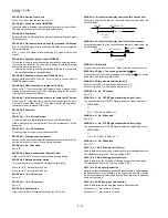
1. Document feed block and diagram

Fig. 1

2. Document feed operation

1) The document placed in the hopper actuates the document sensor.

After one second, the pulse motor starts to drive the paper feed roller.
The document is automatically taken up into the machine, and stopped
at the document sensor.

2) When a specified number of pulses are received from the document

sensor after the document lead edge is sensed, scanning is started.

3) When a specified number of pulses are received from the document

sensor after the document rear edge is sensed, scanning is termi-
nated and the document is fed through.

4) If the document sensor is active (i.e., another document is in the

hopper), when the preceding document scanning is completed and it
is fed out, the next document is taken up into the machine. If the
document sensor is not active (i.e., there is no document in the hop-
per), when the document is fed out, the operation is terminated.

3. Hopper mechanism

3-1. General view

Fig. 2

The hopper is used to align documents with the document guides ad-
justed to the paper width.
NOTE: Adjust the document guide after setting up the document.

3-2. Automatic document feed

1) Use of the paper feed roller and separation rubber plate ensures er-

ror-free transport and separation of documents. The plate spring
presses the document to the paper feed roller to assure smooth feed-
ing of the document.

2) Document separation method: Separation rubber plate

Fig. 3

3-3. Documents applicable for automatic feed

NOTE: Double-side coated documents and documents on facsimile re-

cording paper should be inserted manually. The document feed
quantity may be changed according to the document thickness.

Documents corresponding to a paper weight heavier than 64.3kg (74.3g/
m

2

 ) and lighter than 135kg (157g/m

) are acceptable for manual feed.

Documents heavier than 135kg in terms of the paper weight must be
duplicated on a copier to make it operative in the facsimile.

3-4. Loading the documents

1) Make sure that the documents are of suitable size and thickness, and

free from creases, folds, curls, wet glue, wet ink, clips, staples and
pins.

2) Place documents face down in the hopper.

i) Adjust the document guides to the document size.

ii) Align the top edge of documents and gently place them into the

hopper. The first page under the stack will be taken up by  the feed
roller to get ready for transmission.

NOTES: 1) Curled edge of documents, if any, must be straighten

out.

2) Do not load the documents of different sizes and/or

thicknesses together.

3 – 1

Paper size

B6 (128mm x 182mm) ~
A4 (210mm x 297mm), Letter (216mm x 279mm)

4x6 series
(788mm x 1091mm x
1000mm sheets)

Square
meter series

Minimum

Maximum

Minimum

Maximum

Feeder capacity

10 sheets, max.

Paper thickness (ref.)

0.06mm

0.09mm

0.06mm

0.09mm

Paper weight

45kg

64.3kg

52g/m

2

74.3g/m

2

Fig. 4

Separator rubber

Rear roller A/B

Transfer roller

Pinch roller

CIS

Paper feed roller

Document

Paper feed spring

Separator rubber

Paper feed spring

Document

Paper feed roller

Separator rubber

Paper feed spring

Paper feed roller

Last page of document

First page of document

Back of document

Summary of Contents for FO-375

Page 1: ... 4 Circuit description of power supply PWB 5 11 5 Circuit description of CIS unit 5 11 CHAPTER 6 CIRCUIT SCHEMATICS AND PARTS LAYOUT 1 Control PWB circuit 6 1 2 TEL LIU PWB circuit 6 9 3 Power supply PWB circuit 6 11 4 Operation panel PWB circuit 6 13 CHAPTER 7 OPERATION FLOWCHART 1 Protocol 7 1 2 Power on sequence 7 2 CHAPTER 8 OTHERS 1 Service tools 8 1 2 IC signal name 8 3 PARTS GUIDE CONTENTS ...

Page 2: ...lmistajan ohjeiden mukaisesti French ATTENTION Il y a danger d explosion s il y a remplacement incorrect de la batterie Remplacer uniquement avec une batterie du même type ou d un type recommandé par le constructeur Mettre au rébut les batteries usagées conformément aux instructions du fabricant Swedish VARNING Explosionsfare vid felaktigt batteribyte Använd samma batterityp eller en ekvivalent ty...

Page 3: ...on scheme MH MR Sharp special mode Scanning method Sheet feeder CIS Contact Image Sensor Effective recording width 8 3 210 mm max Input document size Automatic feeding Width 5 8 to 8 5 148 to 216 mm Length 5 5 to 11 140 to 279 mm Manual feeding Width 5 8 to 8 5 148 to 216 mm Length 5 5 to 23 6 140 to 600 mm Effective scanning width 8 3 210 mm max Contrast control Automatic Dark selectable Copy fun...

Page 4: ...the volume of the ringer at all other times 7 STOP key Press this key to stop operation before they are completed 8 Number keys Use these keys to dial numbers and enter number and letters during number name storing procedures 9 SPEED DIAL key Press this key to dial a 2 digit Speed Dial number 10 REDIAL key Press this key to automatically redial the last number dialed 11 SPEAKER key Press this key ...

Page 5: ... 140 279 mm 5 Automatic Document Feeder Capacity Number of pages that can be placed into the feeder at anytime is as follows Normal size max ADF 20 sheets 14 lbs 20 lbs Special size single sheet only manual feed NOTES When you need to send or copy more pages than the feeder limit place additional pages in feeder when last page in feeder is being scanned Place additional pages carefully and gently ...

Page 6: ...tall a surge protector for the power and telephone lines Surge protectors can be purchased at most telephone specialty stores If the machine is moved from a cold to a warm place If the machine is moved from a cold to a warm place it is possible that the reading glass may fog up preventing proper scanning of documents for transmission To remove the fog turn on the power and wait approxi mately 2 ho...

Page 7: ...out blank after printing YES NO 4Insert the leading edge of the paper into the paper inlet Continue to push the paper through the inlet until it comes out of the opening in the front of the fax 5Close the operation panel making sure it clicks into place 6UX 108 A short length of the fax paper will feed out Grasp the paper by the edge and pull upward to tear it off UX 178 UX 188 FO 375 A short leng...

Page 8: ...he paper roll UX 178 188 FO 375 If any pieces of paper are stuck in the cut ter remove them with caution UX 178 188 FO 375 Press the START key to reset the cutter 3Cut off the wrinkled part of the paper 4Reload the paper Jammed fax paper is often caused by improper loading Be sure to carefully follow the instructions for paper loading given in Load ing the Fax Paper in Chapter 1 5If the display st...

Page 9: ...TIME SET Press the START key Enter two digits for the Month 01 through 12 Enter two digits for the Day 01 through 31 Enter four digits for the Year EX 1998 Enter two digits for the Hour 01 through 12 Enter two digits for the Minute 00 through 59 Press the key for A M or the key for P M When finished press STORING AND CLEARING NUMBERS FOR AUTO DIALING 1 Press Display shows FAX TEL MODE 2 Press 1 to...

Page 10: ...PW Pin No 2 1 TEL LIU PWB POWER SUPPLY PWB CNLIU CNLIUA CN2 CNPW CONTROL PWB CONTROL PWB TOP SIDE CNLIUA CNPW FU100 4 Method of release of starting lock up by Battery Reset 1 Summary There is a possibility of release of the lock up by reset the signal BATRST of CPU XFC3 XFC5 if it lock up when you turn on the power of the set in UX 108 series We inform you of the method of release 2 Contents When ...

Page 11: ...compensation is performed in this mode 9 9 ALL BLACK MODE To check the print head whole dots are printed over the interval of 2 m 10 10 AUTO FEEDER MODE Insertion and discharge of document are tested 11 ENTRY DATA SEND Registered content is sent 12 ENTRY DATA RECEIVE Registered content is received and its list is output 13 CUTTER AGING Recording paper is successively cut Cutter model only If the d...

Page 12: ... is used to send various signals to the circuit during FAX com munication Every push of START key sends a signal in the following sequence Moreover the signal sound is also output to the speaker when the line monitor of the soft switch is on 1 No signal CML signal turned on 2 9600bps 3 7200bps 4 4800bps 5 2400bps 6 300bps FLAG 7 2100Hz CED 8 1100Hz CNG 9 END 3 7 Memory clear mode This mode is used...

Page 13: ...the number of cutting times is integrated In the following cases the operation is stopped 1 The stop key is continuously pressed 2 There is no recording paper 3 The recording paper is jammed 4 How to make soft switch setting To enter the soft switch mode make the following key entries in sequence Press FUNCTION 9 8 7 START START Press FUNCTION key Press key Press key Bit1 8 are set Soft SW A2 SW L...

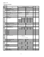
Page 14: ...in RTN No communication error Communication error 0 sending mode reception 8 CNG transmission No Yes 0 CED tone signal interval 1000ms 750ms 500ms 75ms 1 No 1 1 1 0 0 0 2 No 2 1 0 1 0 0 3 MR coding No Yes 0 4 Reserved 0 5 Reserved 0 6 Reserved 0 7 Reserved 0 8 Reserved 0 1 Signal transmission level Binary input 0 2 No 16 8 4 2 1 1 3 1 2 3 4 5 0 4 0 1 0 1 0 10 dBm 1 5 0 6 Protocol monitor error pri...

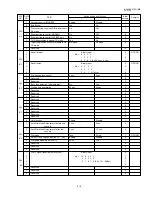
Page 15: ...one detection after auto dial No Yes 1 5 Waiting time after dialing 90 sec 45 sec 0 6 Reserved 0 7 Reserved 0 8 Reserved 0 1 Reserved 0 2 Reserved 0 3 Reserved 0 4 Reserved 0 5 Reserved 0 6 Reserved 0 7 Reserved 0 8 Hold function Enable Disable 1 1 Auto Dial Mode Delay timer of before line 3 sec 0 sec 0 connect 2 Auto Dial Mode Delay timer of after line 3 sec 1 7 sec 0 connect 3 Dial mode Tone Pul...

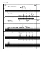
Page 16: ...for auto receive Binary input 0 OPTION 2 No 8 4 2 1 1 3 1 2 3 4 0 4 0 1 0 0 4 times 0 5 Automatic switching manual to auto receive Reception after 5 rings No reception 0 mode 6 Reserved 0 7 Reserved 0 8 Reserved 0 Distinctive ringing setting No 1 No 2 No 3 OPTION Factory setting OFF OFF 0 0 0 STANDARD 0 0 1 1 PATTERN1 0 1 0 0 2 PATTERN2 0 1 1 0 3 PATTERN3 1 0 0 0 4 Reserved 0 5 Caller ID function ...

Page 17: ...1 1 0 3 No 3 0 1 0 1 1 Number of CNG STAND BY mode 1pulse 2pulses 3pulses 4pulses 4 No 4 0 0 1 1 0 5 No 5 0 1 0 1 1 6 Fax signal detection after telephone mode dial Yes No 0 7 Reserved 0 8 Reserved 0 1 Quiet detect time Binary input 0 OPTION 2 No 8 4 2 1 1 3 1 2 3 4 0 4 0 1 0 0 4 sec 0 5 Quiet detect start timing Binary input 0 6 No 8 4 2 1 1 7 5 6 7 8 0 8 0 1 0 1 5 sec 1 1 Reserved 0 2 Reserved 0...

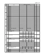
Page 18: ... Fax switching when A M full Yes No 0 OPTION 4 Reserved 0 5 Reserved 0 6 Reserved 0 7 Reserved 0 8 Reserved 0 1 Reserved 0 2 Reserved 0 3 Reserved 0 4 Reserved 0 5 Reserved 0 6 Reserved 0 7 Reserved 0 8 Reserved 0 1 Reserved 0 2 Reserved 0 3 Reserved 0 4 Reserved 0 5 Reserved 0 6 Reserved 0 7 Reserved 0 8 Reserved 0 1 Reserved 0 2 Reserved 0 3 Reserved 0 4 Reserved 0 5 Reserved 0 6 Reserved 0 7 Re...

Page 19: ...ving setting No Yes 1 OPTION Ringer volume Off Low Middle High OPTION 7 No 7 0 0 1 1 1 8 No 8 0 1 0 1 0 Speaker volume Low Low Middle High OPTION 1 No 1 0 0 1 1 1 2 No 2 0 1 0 1 0 3 Polling key Yes No 0 OPTION Handset receiver volume Low Low Middle High OPTION 4 No 4 0 0 1 1 1 5 No 5 0 1 0 1 0 6 Reserved 0 7 Reserved 0 8 Reserved 0 1 Reserved 0 2 Reserved 0 Communication results printout Error Tim...

Page 20: ...d 0 7 Reserved 0 8 Reserved 0 1 Reserved 0 2 Reserved 0 3 Reserved 0 4 Reserved 0 5 Reserved 0 6 Reserved 0 7 Reserved 0 8 Reserved 0 1 Reserved 0 2 Reserved 0 3 Reserved 0 4 Reserved 0 5 Reserved 0 6 Reserved 0 7 Reserved 0 8 Reserved 0 SW l K1 SW l L1 SW l L2 SW NO DATA NO ITEM Switch setting and function 1 0 Remarks Initial setting 2 11 ...

Page 21: ...INT described in the passcode list at the front end of receiver s original when original is sent to the remote machine If this switch is set to NO the HEADER PRINT is not output at the receiving machine SW A2 No 6 H2 mode Used to determine reception of H2 mode 15 sec transmission mode When set to OFF H2 mode reception is inhibited even though the trans mitting machine has H2 mode function SW A2 No...

Page 22: ...on after auto dialing SW B2 No 5 Waiting time after dialing This is waiting time for the opponent s signals after dialing When set to 0 waiting time is 45 sec When set to 1 waiting time is 90 sec SW B2 No 6 No 8 Reserved Set to 0 SW B3 No 1 No 7 Reserved Set to 0 SW B3 No 8 Hold function Used to set YES NO of holding function by the HOLD key SW B4 No 1 Auto dial mode Delay timer of before line con...

Page 23: ...6 No 7 CI off detection timer Distinctive ring setting off only Set the minimum time period of CI signal interruption which affords to be judged as a CI OFF section SW D2 No 8 Reserved Set to 0 SW E1 No 1 No 8 Reserved Set to 0 SW E2 No 1 No 8 Reserved Set to 0 SW F1 No 1 No 2 DTMF detect time Used to set detect time of DTMF Dual Tone Multi Frequency used in remote reception 5 The longer the detec...

Page 24: ...led to prevent accidental wrong input SW J1 No 4 No 5 Reserved Set to 0 SW J1 No 6 Day light saving setting This is used to set YES NO of automatic clock adjustment for day light saving SW J1 No 7 No 8 Ringer volume Used to adjust ringing volume SW J2 No 1 No 2 Speaker volume Used to adjust sound volume from a speaker SW J2 No 3 Polling key If this switch is set to 1 the last of Rapid key works as...

Page 25: ...DIAG mode by pressing SPEED key A bit which is used in the production process only When the SPEED key is pressed the switch is changed from the stand by state to the DIAG mode SW K1 No 2 No 8 Reserved Set to 0 SW L1 No 1 No 8 Reserved Set to 0 SW L2 No 1 No 8 Reserved Set to 0 2 16 ...

Page 26: ...following format and check the related matters TO ATT Ref No CC ATT Date FM Dept Sign 2 17 Please complete this report before calling the TAC hotline if problem still occurs Facsimile communication problem Ref No Date From Mr Fax Tel No Our customer Name Tel No Address Fax No Contact person Model name Other party Name Tel No Address Fax No Contact person Model name Problem mode Line Domestic inter...

Page 27: ...rror occurred just after fallback 13 Error occurred after a response to retransmission end command was received G3 Reception Code Final received signal Error Condition Receiver side 0 Incomplete signal frame Cannot recognize bit stream after flag 1 NSS DCS Cannot recognize CFR or FTT signal Disconnects line during transmission line error 2 NSC DTC Cannot recognize NSS signal FIF code etc 3 EOP Can...

Page 28: ...hod Separation rubber plate Fig 3 3 3 Documents applicable for automatic feed NOTE Double side coated documents and documents on facsimile re cording paper should be inserted manually The document feed quantity may be changed according to the document thickness Documents corresponding to a paper weight heavier than 64 3kg 74 3g m2 and lighter than 135kg 157g m2 are acceptable for manual feed Docum...

Page 29: ...a thermal head permits easier maintenance and low operating costs 1 Thermal head The thermal head consists of 1728 dot heat elements arranged in a sin gle row and has the resolution of 8 dots mm The maximum recording speed is 10ms line The thermal head also incorporates a 1728 dot shift register latch and output control driver circuit Low power consumption is achieved by dividing the head into nin...

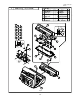
Page 30: ...ction are common to each other To assure reliability of the product the disassembly and the assembly procedures should be performed carefully and deliberately Handset cover and paper support guide 1 Parts list Fig 1 No Part name Q ty No Part name Q ty 1 Mechanism unit 1 2 Handset cover 1 3 Hook switch lever 1 4 Screw ø3 12 2 5 Paper support guide unit 1 6 Anti curl shaft 1 Fig 1 3 3 7 Anti curl sp...

Page 31: ...h cable 1 4 Connector 2 5 Screw 3 10 1 6 PWB case unit 1 7 Screw 3 10 2 8 PWB case top 1 9 Screw 4 6 1 10 AC cord ass y 1 11 Screw 3 6 1 12 TEL ARG cable 1 13 Power supply PWB unit 1 14 TEL LIU PWB unit 1 15 Rubber leg 2 16 PWB case bottom 1 2 3 4 5 6 1 6 13 10 11 12 15 7 7 16 1 8 7 9 10 11 12 13 14 15 16 9 8 AC cord earth cable 45 2 5 3 4 4 Rib 3 Control PWB 14 ...

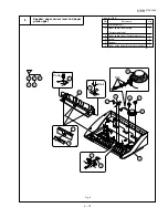
Page 32: ...er 1 5 Reduction gear 17 36Z 1 6 Reduction gear 17 21Z 1 7 Idler gear 25Z 1 8 Feed roller shaft 1 9 Feed roller 1 10 CIS cable 1 11 CIS support right 1 12 CIS unit 1 13 CIS support left 1 14 CIS spring 2 15 Scanner frame 1 16 Panel and head cable 2 17 Operation panel unit 1 2 3 4 5 16 17 1 7 6 8 9 10 11 14 15 12 13 8 4 15 9 8 5 6 14 7 10 14 11 2 2 3 2 3 1 16 16 17 1 13 12 Stopper plate Hook Hook H...

Page 33: ...t 5 Screw 3 10 2 6 Head sheet 1 7 Head cable 1 8 Head spring A 2 9 Head spring B 3 10 Screw 3 6 1 11 Head support right 1 12 Screw 3 6 1 13 Head earth cable 1 14 Head support left 1 15 Thermal head 1 16 Pinch roller shaft 1 17 Pinch roller 2 18 Pinch roller pressing 2 spring 19 Head frame 1 1 4 2 16 2 17 18 18 12 13 14 6 5 9 8 10 11 15 5 3 19 8 7 13 14 B A View A View B 2 3 4 5 6 1 8 7 9 10 11 12 ...

Page 34: ... Transfer roller 1 7 Transfer bearing 1 8 Idler gear 20Z 1 9 Panel lock lever spring 1 10 Panel lock lever 1 11 Document sensor lever 1 spring 12 Document sensor lever 1 13 Separate spring 1 14 Separator plate 1 15 Paper feed spring 1 16 Separator rubber 1 17 Document guide upper 1 2 1 3 4 5 6 8 7 9 10 11 12 13 14 15 16 17 Applying standard Applying standard 12 11 14 13 13 16 15 12 11 9 8 17 1 6 7...

Page 35: ... PWB 1 5 Document tray 1 6 Screw 1 7 Pinion gear 1 8 Hopper spring 1 9 Hopper guide right 1 10 Hopper guide left 1 11 Stop key 1 12 Start key 1 13 Direct key 1 14 12 key 1 15 Operation panel 1 Operation panel PWB LCD cable LCD PWB Confim of HOPPER GUIDE position HOPPER GUIDE R HOPPER GUIDE L 2 3 4 5 6 1 8 7 9 10 11 12 13 14 15 15 1 10 9 8 6 7 5 11 12 13 14 2 2 3 2 4 1 Rib Rib GAP 0 GAP 0 ...

Page 36: ...5 Platen gear 1 6 Platen roller 1 7 Platen bearing 2 8 Screw 3 10 1 Cutter model only 9 Cutter unit 1 Cutter model only 10 Screw 3 10 1 Cutter model only 11 Cutter cover 1 Cutter model only 12 Cutter guide 1 Cutter model only 13 Cutter 1 Cutter model only 14 Screw 3 10 2 15 Speaker cable 1 16 Control PWB unit 1 2 3 4 5 16 1 7 6 8 9 10 11 14 15 12 13 1 5 7 6 1 2 2 4 2 4 2 15 14 14 16 6 16 7 3 5 7 8...

Page 37: ... Cutter model only 3 Paper sensor lever Cutter model only 1 4 Screw 2 5 Speaker 1 6 Paper guide upper Non cutter model only 1 Parts list Fig 8 No Part name Q ty Fig 8 Speaker paper sensor lever and paper guide upper 8 3 10 2 3 4 5 1 1 2 3 4 4 5 6 1 1 5 1 6 2 3 Rib Hook Hook 6 ...

Page 38: ...net gear spring 1 11 Planet gear lever B 1 12 Idler gear 25Z 1 13 Cam switch 1 14 Reduction gear 17Z 1 15 Idler gear 25Z 1 16 Screw 3 10 1 17 Motor 1 18 Motor heat sink 1 19 Drive frame 1 1 2 3 4 5 6 9 19 7 10 8 11 13 12 14 15 16 17 18 16 19 13 17 18 19 13 14 6 7 8 11 9 10 15 4 12 2 1 1 3 3 5 10 7 To be the switch linked by hooks Grease Grease Green Lock the MOTOR by this rib SECTION A A A A Hook ...

Page 39: ...1 16 Planet gear lever B 1 17 Idler gear 25Z 1 18 Cam switch 1 19 Reduction gear 17 30Z 1 20 Reduction gear 17 30Z 1 21 Reduction gear 17 36Z 1 22 Idler gear 25Z 1 23 Idler gear 25Z 1 24 Idler gear 20Z 1 25 Screw 3 10 1 26 Motor 1 27 Motor heat sink 1 28 Drive frame 1 1 2 5 8 9 10 11 14 3 6 12 15 4 7 13 16 18 17 19 20 21 22 23 24 25 26 27 28 25 28 1 18 26 27 1 28 18 21 11 12 13 16 14 15 24 23 8 17...

Page 40: ... 20 5mm Head head earth and panel cable Head cable Motor cable Brinding the cable Head cable Head earth cable CIS cable panel cable motor cable cam cable Head cable and head earth cable Head earth cable Head cable Operation panel PWB Panel cable Panel cable CIS cable CIS cable CIS unit Speaker cable 1 6 1 1 1 5 1 6 5 Postion of core Panel cable pass to the core 2times The panel cable mustwiring to...

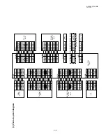
Page 41: ...LCD CONTROL PWB UNIT 1CHIP FAX ENGINE XFC 3 HANDSET SPEAKER 5V 24V OPERATION PANEL TEL LIU PWB UNIT DRIVER THERMAL HEAD PM CONTACT IMAGE SENSOR DOCUMENT SENSOR POWER SUPPLY PWB UNIT PAPER SENSOR AND CUTTER UX 178U 188U FO 375U ONLY AMP SIGNAL SELECT BLOCK SPEAKER AMP AMP AMP SURGE PROTECT FILTER CML TRANS CI VBT REGULATOR RECTIFIER TRANS RECTIFIER DIODE TRANS SURGE ABSORBER FILTER STABILIZER LINE ...

Page 42: ...NTACT IMAGE SENSOR LCD UNIT CNLCD OPERATION PANEL PWB 14 CNPN 16 7 15 CNCSW CNMT CNTH CNCIS CNPN CNSP SPEAKER CNCUT1 CNLIUA CNPW 12 10 CONTROL PWB UNIT TEL LIU PWB UNIT POWER SUPPLY PWB UNIT CNLIU CN2 EXTERNAL LINE TEL LINE MJ1 2 MJTEL AC CORD UX 178U 188U FO 375U ONLY TX RX MOTOR 2 HANDSET FG ...

Page 43: ...G 5V øT CISCLK GLED 24V VO DG 5V øT CISCLK GLED 24V KEN4A KEN3A KEN2A KEN1A DG DG 5V ORGSNS FRSNS E SEN4 SEN3 SEN2 SEN1 SEN0 KEN4A KEN3A KEN2A KEN1A DG DG 5V ORGSNS FRSNS E SEN4 SEN3 SEN2 SEN1 SEN0 CNPN CNPN CNCIS 1 2 3 4 5 6 7 8 9 10 11 12 1 2 3 4 5 6 7 8 9 10 11 12 TEL LIU PWB TELOUT TELIN TELMUTE CI HS RHS RXIN TXOUT CML 24VA 5V DG TELOUT TELIN TELMUTE CI HS RHS RXIN TXOUT CML 24VA 5V DG CNLIU ...

Page 44: ...ed in the transmit buffer of the RAM The data is then con verted from parallel to serial form by the modem where the serial data is modulated and sent onto the line Receive operation There are two ways of starting reception manual and automatic Depression of the START key in the off hook mode in the case of manual receive mode or CI signal detection by the LIU in the auto matic receive mode First ...

Page 45: ...A CONTROLLER OPERATOR PANEL IF 32 KEYS 8 LEDS LCD MODULE SYNC SERIF 1 THERMAL PRINTER IF 5 ms LINE TIME A4 B4 LINES TPH ADC 4 STROBE TPH LATCHLESS TPH EXTEMAL DMA I F T 4 T 6 CODEC MH MR MMR HARDWARE ALTERNATE COMPRESSION DECOMPRESSION BI LEVEL RESOLUTION CONVERSION PROGRAMMABLE REDUCTION EXPANSION 2 6kBYTE VIDEO RAM SCANNER CONTROL VIDEO PROCESSING 8 BIT PADC CCD CIS SCANNER 5 ms A4 B4 LINES SHAD...

Page 46: ...f VDD power Scanner Interface START 101 O 2XS Scanner shift gate control CLK1 100 O 2XS Scanner clock CLK1n 99 O 2XS Scanner clock inverted CLK2 98 O 2XS Scanner reset gate control or clock for CIS scanner FCS1n VIDCTL0 96 O 2XT Flash memory chip select or Video Control signal FCS2n VIDCTL1 97 O 2XT Flash memory chip select or Video Control signal Printer Interface PCLK 29 O 3XC Thermal Print Head...

Page 47: ...teresis In GPIO 13 or I O chip select 3 GPIO 14 CS 4 n 78 I O H 2XC Hysteresis In GPIO 14 or I O chip select 4 GPIO 15 CS 5 n 77 I O H 2XC Hysteresis In GPIO 15 or I O chip select 5 GPIO 16 IRQ 8 76 I O H 1XC Hysteresis In GPIO 16 or external interrupt 8 GPIO 17 IRQ 5 n 75 I O H 1XC Hysteresis In GPIO 17 or external interrupt 5 GPIO 18 IRQ 9 n 74 I O H 1XC Hysteresis In GPIO 18 or external interru...

Page 48: ... START CLK2 CLK1 CLK1N VIDCTL 1 0 XIN XOUT MIRON MCSN SYSCLK D 7 0 RDN A 4 0 WRN MONOFAX FACSIMILE MODEM ANALOG SWITCH LINE INTERFACE SPEAKER MICROPHONE CIRCUIT TELEPHONE LINE RXA TXA SPKR MIC RIN SPKRLO SPKRHI SPKR RIN TXA2 TXA1 TXOUT RXIN XIA GPIO DRAM OPTION SCANNER VIDEO PREPROCESSING SYNC PORTS 2 SSIF VIN VREF VREF SSCLK 2 1 SSTXD 2 1 SSRXD 2 1 SSSTAT 2 1 SYNC ASYNC SERIAL PORT SASCLK SASTXD ...

Page 49: ...her a 100 pin plastic quad flat pack PQFP or a 64 pin quad in line package QUIP General purpose input output GPIO pins are available for host as signment in the 100 pin PQFP The modem s small size single voltage supply and low power con sumption allow the design of compact system enclosures for use in both office and home environments MONOFAX is a registered trademark of Rockwell International FEA...

Page 50: ...48 AGD R 49 AOUT R 50 0VD1 GND 51 NC 52 IRQ OC 53 WRITE R W IA 54 CS IA 55 READ φ2 IA 56 RS4 IA 57 RS3 IA 58 RS2 IA 59 RS1 IA Pin No Signal Name I O Type 60 RS0 IA 61 GP13 IA OB 62 NC 63 GP11 IA OB 64 RTS IA 65 EN85 R 66 0VD2 GND 67 PORI ID 68 XTLI R 69 XTLO R 70 XCLK OD 71 YCLK OD 72 5VD1 PWR 73 DCLK1 R 74 SYNCIN2 R 75 GP16 IA OB 76 GP17 IA OB 77 0VD2 GND 78 CTS OA 79 TXD IA 80 0VD2 GND 81 0VD2 G...

Page 51: ...he CML relay is turned on and off for control in the DP calling system Refer to the attached sheet DTM transmission It is formed in the modem and is output 3 Speaker amplifier section The volume of the ringer sound speaker sound is controlled with 2 bit signal of VOLA and VOLB and the sound switch is controlled with BZ CONT 4 Ringer circuit section The ringer sound is formed in the tone of 1 chip ...

Page 52: ...ncel Normal operation Handset reception mute control signal TEL MUTE H Muting L Muting cancel Handset receiver volume control signal RCVOL1 RCVOL2 The circuit is located in the control PWB Three stage switching Note The DTMF sending listed above is DTMF signal sending in the handset OFF HOOK mode Speaker volume control signal VOL A VOL A VOL B matrix VOL B The circuit is located in the control PWB...

Page 53: ...ok state Signals for status recognition according to input signals Signal Name Function TEL IN Receiving signal from line or modem TEL OUT Transfer signal to line SPOUT Speaker output signal TXOUT Transmission DTMF analog signal output from modem RXIN Reception DTMF others analog signal input into modem Other signals CONTROL PWB TEL LIU PWB TEL LINE EXT HANDSET SPEAKER H L TX OUT RX IN 1 0 0 1 HS ...

Page 54: ...contact with the full size sensor for scanning being a monochromatic type with the pixel number of 1 728 dots and the main scanning density of 8 dots mm It is composed of sensor rod lens LED light source light conductive plate control circuit and so on and the reading line and focus are previously adjusted as the unit Due to the full size sensor the focus distance is so short that the set is chang...

Page 55: ...kHz C4 4 7 50 R126 100K C5 10 50 DG 17 18 A9 A8 A7 A6 A5 A4 A2 A1 A0 RD WR ROMCS CS1 MCS SYNC REGDMA WAIT RAS CAS0 CAS1 DWR WRPROT A B A16 A15 A14 A13 A12 A11 A10 A9 A8 A7 A6 A5 A4 A3 A2 A1 A0 32 DG C129 1 5V C DG H I J RA3 470 x 4 90 GPIO4 100 CLK1 30 PDAT 24 A3 D E F G 57 CS0 K GPIO3 GPIO2 GPIO1 GPIO0 10K 10K 10K 10K 10K 10K R106 10K R130 3 3K 10K 1 RA1 RA1 RA1 3 2A MDMRST 4 4C CUT1I CNLIUB 4 CN...

Page 56: ...2 IO4 15 A11 24 A11 IO3 13 A10 25 A10 IO2 12 A9 3 A9 IO1 11 A8 4 A8 A7 5 A7 A6 6 A6 A5 7 A5 VDD 28 A4 8 A4 VSS 14 A3 9 A3 A2 10 A2 A1 A0 20 A0 27 WE 22 CS2 OE A 16 0 1 5I D 7 0 1 6I 1 3I RD 1 3I 5V DG C140 0 1 D7 D6 D5 D4 D3 D2 D1 D0 IC8 27C010 2 A16 DQ8 3 A15 DQ7 A14 DQ6 A13 DQ5 4 A12 DQ4 A11 DQ3 A10 DQ2 A9 DQ1 A8 5 A7 6 A6 A17 7 A5 VCC 8 A4 VPP 9 A3 A2 A1 GND A0 E G IC5 SRM2B256SLMX70 A1 CS1 D7 ...

Page 57: ...0 SWGAIN1 N C N C N C 17 21 30 43 47 C109 0 1 35 87 98 37 45 49 18 48 42 44 88 99 24 19 27 29 31 32 C3 47 25 R136 3 5V R114 0 MAG N C 33 SIGRX 5 4 3 2 1 100 63 38 39 40 R132 85 25 83 26 74 84 86 90 68 GP07 GP06 GP05 GP04 GP03 GP02 GP11 TXLOSS2 TXLOSS1 EYECLK ECLKIN1 EYESYNC SYNCIN1 SYNCIN2 EYECLKX EYEX EYEY XTLI RCVOL1 RCVOL2 VOLA 6 1H CNLIUB 5 6 1H 6 2A 6 2A R135 MAG X1 24 00014MHz C107 18P R110 ...

Page 58: ...RGSNS1 DG C152 0 1 8 4 DG DG 1 4A DRSNS1 1 4A 1 5A 1 4A CNPN 9 FRSNS CNCSW 1 CSW CNCUT1 1 CUT1 C124 0 1 R145 470 DG C133 0 1 R171 Z2139 DG C151 0 1 R206 470 DG C139 DG FRSNS1 CSWI CUT1I DG SW1 DOOR SW 1 4A PSNSI 5V R100 1 1 3 2 4 PI1 DG DG PSNS DG DG HOLBAT 1 BT R228 5 6K CNPW 2 5V HOLBAT 2 BT HOLBAT 3 DG BAT1 CR2032 DG D101 RB705D 5V DG C159 0 1 VBT VBT 5V CNPW 1 DG DG CNLIUA 11 5V CNLIUA 12 DG C...

Page 59: ...3 5V CNCIS 2 DG CNCIS 7 24V CNCIS 6 GLED C142 1 R188 IC10 2904 6 5 7 R209 R217 R210 R227 R1 R235 Q1 Q103 E B C DG DG DG 1 1E VREFCONT 5 5H LEDON COM 9 1 1B 1C 16 2 2B 2C 15 3 3B 3C 14 4 4B 4C 13 5 5B 5C 12 6 6B 6C 11 7 7B 7C 10 8 E TPA TPB 1 1E TPA 1 1E TPB 1 1E 1 1E 1 4A VTHON 3 1D LEDON IC7 ULN2003A VMT CNMT 5 VMT CNMT 6 TPAD CNMT 1 TPBD CNMT 2 TPAD CNMT 3 TPBD CNMT 4 VTHON CNPW 3 LEDON 5 1B 24V...

Page 60: ...78 3 3K R177 62K R175 0 EXSIG CNLIUB 1 C145 0 1 R180 N M RCVOL1 3 1C R222 47K 14 13 12 IC4 4066 24VA R219 1 5K C154 0 1 R223 47K R220 10K TELIN CNLIUA 2 DG DG C155 1000P DG C156 0 1 11 4 RCVOL2 CNLIUB 2 RCVOL1 CNLIUB 6 DG VREF 5V C148 0 1 RCVOL2 3 1C R211 33K R165 30K R164 2K IC4 4066 IC9 2902 13 1 2 5 3 4 R213 33K C153 1 2 15 1 10 IC6 4053 0 1 DG R179 1K DG C143 4700P IC4 4066 R141 10K R138 47K I...

Page 61: ...6 7 UX 108U 178U 188U FO 375U Control PWB parts layout Top side ...

Page 62: ...6 8 UX 108U 178U 188U FO 375U Control PWB parts layout Bottom side ...

Page 63: ...U 8 TXOUT C11 4 7 50 R17 10K C4 2200P 2 3 1 R16 10K R10 10K R9 10K C3 2200P VREF CNLIU 7 RX IN ZD3 HZ27 PC2 TLP521 1 CNLIU 9 CML B E CNLIU 11 IC1 2904 8 4 MJTEL 1 TX C14 4 7 50 R11 1 5K L6 MJTEL 4 TX MJTEL 3 RX C1 2200P CNLIU 1 TELOUT 5 C16 1000P R12 1K C13 2 2 50 R15 3 3K R14 15K C18 3300P L7 N2024 MJTEL 2 RX D1 1SS270 E R1 CNLIU 3 TEL MUTE N M CNLIU 10 CNLIU 12 24V 5V VA1 VA2 R8 JP C20 N M R20 1...

Page 64: ...6 10 UX 108U 178U 188U FO 375U TEL LIU PWB parts layout ...

Page 65: ...0FB3 R19 R12 2 2K Q3 2SC1740S PC1 PS2501 1 R13 270 R14 3 9K VR1 470 R15 120 7 10 VM IC1 BA178M05T 1 3 2 C18 470 16 D8 SR140 R10 22 D6 IS2076A PC1 PS2501 1 1 2 C4 AC L AC N R3 8 2k C9 0 068 R4 100 Q4 2SC1741AS Q2 2SC2655 Y C10 1000P C11 1000P ZD2 RD3 9ESAB2 R9 680 R8 680 C8 0 01 C12 4700P C17 6 MG VTH MG MG 5 4 5V 2 DG 1 CN2 3 1 R1 560K C3 V2 D3 D2 D4 D1 TH1 8 2ohms N M C13 3300P R6 680 R11 680 C14...

Page 66: ...6 12 UX 108U 178U 188U FO 375U Power supply PWB parts layout ...

Page 67: ...1 74HC147 CNLCD 6 CNLCD 5 CNLCD 3 CNLCD 2 CNLCD 1 C2 22 50 C1 0 022 CNLCD 11 LD4 CNPN 4 GND CNLCD GND 1 2 3 4 5 6 7 8 9 10 11 12 13 14 5V VO RS GND E N C N C N C N C LD4 LD5 LD6 LD7 CNPN KEN 4A KEN 3A KEN 2A KEN 1A 5V GND GND ORGSNS FRSNS E SEN4 SEN3 DOWN 01 UP 02 STOP START 5 REC 9 3 6 HOLD SPEAKER SPEED REDIAL 07 09 03 05 08 10 04 06 7 1 4 D5 1SS270 D4 1SS270 D3 1SS270 D1 1SS270 CNLCD 12 LD5 CNL...

Page 68: ...I CSI TSI RTC EOP MCF DCN IMAGE SIGNAL Document ejected Recording papor ejected Receive side G3 communication CED Transmitter side Document inserted into document sensor during standby To recording position DCS Cut line printed IMAGE SIGNAL Cut line printed IMAGE SIGNAL IMAGE SIGNAL Next page insert command 1st page Document inserted to the reading position DCS ...

Page 69: ...lized MODEM initialized STOP key WAIT A MOMENT display START NO YES STAND BY 3 sec NO MEMORY CLEAR display NO YES STAND BY 3 sec NO NO START key COPY key STOP key NO Memory clear STAND BY 2 1 MEMORY CLEARED display Memory clear PROCESS CHECK MODE MEMORY CLEARED display YES ...

Page 70: ...1 AW 3 C C N W 4 7 5 8 S C 0 1 CIS RELAY CABLE 1 AQ 4 C C N W 4 7 5 9 S C 0 1 HEAD RELAY CABLE 1 AX 5 C C N W 4 7 6 0 S C 0 1 CAM SWITCH RELAY CABLE 1 AK 6 C C N W 4 7 6 1 S C 0 1 CUTTER SWITCH RELAY CABLE 1 AK 7 C C N W 4 7 6 3 S C 0 1 MOTOR RELAY CABLE 1 AP 8 Q C N W 4 7 6 4 S C Z Z PAPER SENSOR RELAY CABLE 1 BB 9 V H P R P i 5 7 4 PHOTO TRANSISTOR PSNS 1 AF 10 V R S T S 2 A D 2 2 1 J RESISTOR 1...

Page 71: ...The setting is as follows The recording paper sensor PSNS is operated by OR of the mechani cal unit switch and the test PWB switch When performing installation in the machine unit set the test PWB switches to the fixed position Mechanical unit PWB to be tested Actual operation with mechanical unit Recording paper sensor ON OFF operation OFF Photo interrupter is interrupted PWB sensor check Recordi...

Page 72: ...and black basis is applied to remember the shading wave form Be sure to perform this operation when replacing the battery or replacing the control PWB Execute in the shading mode of DIAG mode UX 108 178 SERIES SHADING WAVE MEMORY STANDARD PAPER PSHEZ3354SCZZ ...

Page 73: ... 8 1B 2B 3B 4B 5B 6B 7B E 1C 2C 3C 4C 5C 6C 7C COM Signal A0 A12 CE1 CE2 WE OE I O1 I O8 VCC GND N C Address input Chip enable Write enable Write enable Data I O Power source Ground No connection 1 2 3 4 5 6 7 8 9 10 11 12 13 14 A14 A12 A7 A6 A5 A4 A3 A2 A1 A0 DQ1 DQ2 DQ3 GND 28 27 26 25 24 23 22 21 20 19 18 17 DQ5 DQ6 DQ7 DQ8 S1 A10 S2 A11 A9 A8 A13 W VCC TOP VIEW 16 15 DQ4 Pin name 6 11 10 9 12 ...

Page 74: ...OUT 6 CONT C 13 11 9 CONT A IN OUT OUT IN VCC OUT IN IN OUT SWA OUT IN IN OUT SWD IN OUT OUT IN SWB IN OUT OUT IN SWC 1 2 M R SUB 5 VCC TOP VIEW 3 GND 4 VOUT 1 2 3 4 5 6 7 8 9 10 11 12 13 VPP A16 A15 A12 A7 A6 A5 A4 A3 A2 A1 A0 DQ1 32 31 30 29 28 27 26 25 24 23 22 21 20 VCC PGM NC A14 A13 A8 A9 A11 G A10 E DQ8 DQ7 14 15 16 DQ2 DQ3 GND DQ6 DQ5 DQ4 19 18 17 TOP VIEW Pin name A0 A16 E G GND PGM DQ1 D...

Page 75: ...Sn EN85n 0VD2 PORin XTLI XTLO XCLK YCLK 5VD1 24 100 99 98 97 96 95 94 93 92 91 90 89 88 87 86 85 31 32 33 34 35 36 37 38 39 40 41 42 43 44 45 46 57 58 59 60 61 62 63 64 65 66 67 68 69 70 71 72 23 22 21 20 19 18 17 16 15 14 13 12 11 10 9 8 7 6 5 4 3 2 1 D7 0VD2 0VD2 GP07 GP06 GP05 GP04 GP03 DCLKI IRQ2n 73 SYNCIN2 G2XCLK 74 GP16 75 GP17 76 0VD2 77 CTSn 78 TXD 79 0VD2 80 ECLKIN1 25 SYNCIN1 26 NC 27 N...

Page 76: ...0 51 52 VSSI 53 VSSO 72 LCDCS GPIO17 54 55 REGDMA 124 VDDI 123 122 121 120 119 118 117 116 115 114 RASN 113 CAS0N 112 CAS1N 111 110 125 MCSN ROMCSN PM3 GPO3 VDRAM WRPROTN WAITN CSIN TONE CS0N 57 TEST 58 XIN 59 XOUT 60 BATRSTN 61 PWRDWNN 62 VBAT 63 VSSI 64 THADI 65 VREF CLREF 66 VIN 67 ADXG 68 ADGA 69 ADGD 56 ADVA 70 VREF 71 PLAT 31 VDDI 32 STRB3 33 STRB2 34 STRB1 35 STRB0 36 78 77 76 75 GPIO18 IRQ...

Page 77: ...s specifi to the product specification 1 Cabinet etc 2 Upper cabinet 3 Document guide upper 4 Drive unit Non cutter model UX 108 5 Drive unit Cutter model UX 178 188 FO 375 6 Packing material Accessories 7 Control PWB unit 8 TEL Liu PWB unit 9 Power supply PWB unit 50 Hardware parts Index UX 108 UX 178 UX 188 MODEL FO 375 Non Cutter model Cutter model UX 108 UX 178 188 FO 375 ...

Page 78: ... B4 B4 B4 B4 B1 B1 B4 B4 B4 B4 B4 48 42 37 33 28 34 31 32 30 38 35 39 29 29 22 24 55 36 25 23 54 21 10 17 13 20 19 43 18 8 56 45 51 52 53 47 44 44 49 9 6 10 2 58 2 7 11 14 1 5 4 3 3 26 27 B4 B4 15 DOCUMENT GUIDE UPPER NON CUTTER MODEL CUTTER MODEL DRIVE UNIT CUTTER MODEL CUTTER MODEL 59 60 ...

Page 79: ...tch lever 28 LFRM 2185XHZZ AH N C Scanner fram 29 MSPRC2948XHZZ AC N C CIS spring 30 NGERH2379XHZZ AC N C Idler gear 25Z 31 NGERH2380XHZZ AC N C Reduction gear 17 36Z 32 NGERH2392XHZZ AC N C Reduction gear 17 21Z 33 NROLR2375XHZZ AL N C Feed roller 34 NSFTZ2273XHZZ AF N C Feed roller shaft 35 PGIDP2513XHZZ AH N C CIS support left 108U PGIDP2499XHZZ AD N C CIS support left 178U 188U 375U 36 PGIDP25...

Page 80: ...UX 108U 178U 188U FO 375U 3 2 Upper cabinet 3 Document guide upper 14 11 2 1 3 5 4 12 10 8 7 9 6 B2 B3 B3 13 3 2 7 5 6 4 9 15 10 16 1 14 13 12 1 11 8 ...

Page 81: ...ZB AE N C Hopper guide right 375U 11 HPNLH2383XHZB AK N D Decoration panel 108U HPNLH2383XHZA AK N D Decoration panel 178U HPNLH2383XHZD AK N D Decoration panel 188U HPNLH2383XHZC AD N D Decoration panel 375U 12 QCNW 4816XHZZ AL N C Panel cable 13 DCEKP367BXH01 BH N E Operation panel PWB unit 14 LBNDJ2006XHZZ AA C Band Unit 901 DCEKP370BXH01 BL N E Operation panel unit 108U 178U DCEKP370BXH05 BF N...

Page 82: ...FO 375U 5 4 Drive unit Non cutter model UX 108 5 Drive unit Cutter model UX 178 188 FO 375 19 2 1 16 18 12 13 12 13 11 9 6 3 11 4 8 5 8 13 B4 19 2 17 18 1 16 18 12 13 14 11 15 12 13 13 8 7 15 11 9 6 3 11 10 4 8 5 8 13 B4 ...

Page 83: ...h 19 RMOTZ2134XHZZ BA N B Motor 5 Drive unit Cutter model UX 178 188 FO 375 1 LFRM 2186XHZZ AH N C Drive unit frame 2 LPLTM2910XHZZ AE N C Motor heat sink 3 MCAMP2024XHZZ AE N C Cam 4 MLEVP2266XHZZ AD N C Planet gear lever A 5 MLEVP2267XHZZ AD N C Planet gear lever B 6 MLEVP2268XHZZ AD N C Change lever A 7 MLEVP2270XHZZ AD N C Planet gear lever C 8 MSPRC2955XHZZ AC N C Planet gear spring 9 MSPRT29...

Page 84: ...BM4321XHZZ AD N D Box label 108U TLABM4322XHZZ AD N D Box label 178U TLABM4437XHZZ AD N D Box label 188U 5 DUNTK369BXHSG AV N E Handset 108U 178U DUNTK369BXHBE BE N E Handset 188U DUNTK369BXHOG AP N E Handset 375U 6 QCNW 3975XHGY AG C Telephone line cord 7 QCNW 3976XHAG AH C Handset cord 108U 178U QCNW 3976XHBE AT C Handset cord 188U QCNW 3976XHOG AT C Handset cord 375U 8 SPAKP3385SCZZ AG D Vinyl ...

Page 85: ... C Capacitor 50WV 22PF C128 39 VCKYTV1CF105Z AB C Capacitor 16WV 1 0µF C129 40 VCKYTV1CF105Z AB C Capacitor 16WV 1 0µF C131 41 VCKYTV1CF105Z AB C Capacitor 16WV 1 0µF C132 42 VCKYTV1EB104K AA C Capacitor 25WV 0 1µF C133 43 VCKYTV1EF104Z AA C Capacitor 25WV 0 1µF C134 44 VCKYTV1HB103K AB C Capacitor 50WV 0 01µF C135 45 VCKYTV1EF104Z AA C Capacitor 25WV 0 1µF C136 46 VCKYTV1EB104K AA C Capacitor 25W...

Page 86: ...A C Resistor 1 10W 10KΩ 5 R102 121 VRS TS2AD103J AA C Resistor 1 10W 10KΩ 5 R103 122 VRS TS2AD103J AA C Resistor 1 10W 10KΩ 5 R104 123 VRS TS2AD471J AA C Resistor 1 10W 470Ω 5 R105 178U 188U 375U 124 VRS TS2AD303J AA C Resistor 1 10W 30KΩ 5 R106 178U 188U 375U 125 VRS TS2AD471J AA C Resistor 1 10W 470Ω 5 R109 126 VRS TS2AD121J AA C Resistor 1 10W 120Ω 5 R110 127 VRS TS2AD201J AG C Resistor 1 10W 2...

Page 87: ... R211 199 VRS TS2AD562J AA C Resistor 1 10W 5 6KΩ 5 R212 200 VRS TS2AD333J AA C Resistor 1 10W 33KΩ 5 R213 201 VRS TS2AD271J AA C Resistor 1 10W 270Ω 5 R214 202 VRS TS2AD303J AA C Resistor 1 10W 30KΩ 5 R215 203 VRS TS2AD302J AA C Resistor 1 10W 3 0KΩ 5 R216 204 VRS TS2AD303J AA C Resistor 1 10W 30KΩ 5 R217 178U 188U 375U 205 VRS TS2AD103J AA C Resistor 1 10W 10KΩ 5 R218 206 VRS TS2AD152J AA C Resi...

Page 88: ...Transistor 2SC1815GR Q2 36 VSDTC114ES 1 AB B Transistor DTC114ES Q3 37 VRD HT2EY151J AA C Resistor 1 4W 150Ω 5 R2 38 VRD HT2EY300J AA C Resistor 1 4W 30Ω 5 R3 39 VRD HT2EY910J AA C Resistor 1 4W 91Ω 5 R4 40 VRD HT2HY223J AA C Resistor 1 2W 22KΩ 5 R5 41 VRD HT2EY223J AA C Resistor 1 4W 22KΩ 5 R6 42 VRD HT2EY103J AA C Resistor 1 4W 10KΩ 5 R9 43 VRD HT2EY103J AA C Resistor 1 4W 10KΩ 5 R10 44 VRD HT2E...

Page 89: ...0S Q3 36 0CBUAC0264AZ AD N B Transistor 2SC1741AS QR Q4 37 0CBUEEB564CS AC N C Resistor RD16S 564J R1 38 0CBUEFER18CH AD C Resistor SPRX2 R18J R2 39 0CBUEEB822CS AC N C Resistor RD16S 822J R3 40 0CBUEEB101CS AC N C Resistor RD16S 101J R4 41 0CBUEEB184CS AC N C Resistor RD16S 184J R5 42 0CBUEEB154CS AC N C Resistor RD16S 154J R6 43 0CBUEFE823CG AC C Resistor RSS2 823J R7 44 0CBUEEB681CB AC N C Resi...

Page 90: ...8 AD C NROLP2332XHZZ 1 48 AD C NROLP2334XHZA 1 4 AC N C NROLR2372XHZZ 3 12 AL N C NROLR2373XHZZ 3 13 AL N C NROLR2374XHZZ 3 14 AP N C NROLR2375XHZZ 1 33 AL N C NROLR2376XHZZ 1 49 AX N C NSFTZ2273XHZZ 1 34 AF N C NSFTZ2274XHZZ 1 50 AK N C NSFTZ2281XHZZ 1 5 AD N C P PCUSK2113XHZZ 6 13 AG N C PCUT 2037SCZZ 1 51 AT N C PGIDP2496XHZZ 1 42 AD N C PGIDP2497XHZZ 1 6 AC N C PGIDP2498XHZZ 1 7 AC N C PGIDP24...

Page 91: ...N B VHIPST596CMT1 7 107 AF B VHIR96XFC3CID 7 96 BR N B 7 97 BR N B VHIULN2003AN 7 101 AE B VHIW24257S7LL 7 99 AP B VHI27010FWR0F 7 102 BA B VHI27010FWS0F 7 102 BA B VHPITR9606 1 7 112 AG N B VHPPC814X 1 8 32 AE B VHPTLP521 1BL 8 33 AE B VHVERZV5D471 8 59 AC B 8 60 AC B VHVICPS07 1 7 94 AA B VHVRA391PV6 1 8 1 AE B VRD HT2EY102J 8 45 AA C 8 51 AA C 8 56 AA C VRD HT2EY103J 8 42 AA C 8 43 AA C 8 49 AA...

Page 92: ...CODE No NEW MARK PART RANK PRICE RANK PARTS CODE 0CBPHZ0184ZZ 9 53 AR N B 0CBPJCSX2501 9 27 AH A 0CBPKZ0194ZZ 9 16 AC C 0CBPKZ1105ZZ 9 17 AH N C 0CBPZZ0906ZZ 9 28 AH N A 0CBUAC0027CZ 9 34 AG B 0CBUAC0034EZ 9 35 AE B 0CBUAC0264AZ 9 36 AD N B 0CBUAG0166BZ 9 33 AQ N B 0CBUBA0003BZ 9 23 AD N B 9 26 AD N B 0CBUBC0169CZ 9 22 AF N B 0CBUBC0215CZ 9 18 AD N B 9 19 AD N B 9 20 AD N B 9 21 AD N B 0CBUBC0302A...

Reviews: