background image

7

LC-45GD5U

Pa

rt

 names

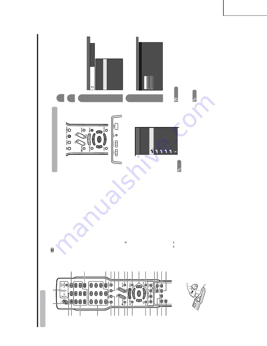
Remote contr

ol unit

2

31

8

19

20

21

22

23

24

25

26

27

28

29 30

31

32

11

7

4

5

6

7

8

9

11

12

13

14

15

16

10

6

AIR:

 Receives air signal.

7

CABLE: 

Receives cable signal.

8

VOL

+

/

-

Sets the volume. 

9

 Vir

tual:


Selects

 V

ir

tual Dolby Surr

ound settings. 

10

INFO:


Displays the pr

ogram infor

mation scr

een. 

11

RECORD:


Recor

ds the pr

ogram to equipment (capable of

recor

ding). 

In TV Guide On Scr

een, initiates the r

ecor

ding pr

ocess.

12

EXIT

Tu

rns of

f the menu screen and TV Guide On

Scr

een.

13

F

A

V

ORITE CH

A

B

C

D:


Selects four pr

eset favorite channels in four

dif

fer

ent categories. 

While watching, you can toggle the selected channels

by pr

essing A, B, C and D.

DA

Y

 /

D

A

Y


In TV Guide On Scr

een, moves forwar

d

or backwar

d in 24 hour incr

ements in the listing grid.

14

A

UDIO:

 Selects the MTS/SAP or the audio mode during

multi-channel audio br

oadcasts. 

15

SLEEP:

 Sets the sleep timer

16

i.LINK: 

Displays the i.LINK panel. 

17

FUNCTION:


Switches the r

emote contr

ol for TV

, CBL/

SA

T

, VCR, DVD and AUDIO operation. Indicator lights

up for the curr

ent mode. 

* T

o

 enter the code r

egistration mode, you need to pr

ess

FUNCTION

 and 

DISPLA

Y

 at the same time.

18

LIGHT 

:

 When pr

essed all buttons on the r

emote

control unit will light. The lighting will tur

n of

f if no

operations ar

e per

for

med within about 5 seconds. This

button is used for per

for

ming operations in low-light

situations.

19

VIEW MODE:


Selects the scr

een size. 

20

ENT

Enters a channel selection when choosing with

the 

0-9

 buttons.

21

FLASHB

A

CK:


Retur

ns to the pr

evious channel or

exter

nal input mode. 

22

INPUT

:

 Selects a Liquid Cr

ystal T

elevision input sour

ce.

(TV

, CableBox, INPUT 1, INPUT 2, INPUT 3, INPUT 4,

INPUT 5, i.LINK)  

If the CableBox is set up in the TV Guide On Scr

een

setting menu, the CableBox option appears.

23

CH


/

Selects the channel.

In the TV Guide On Scr

een, moves one page up or one

page down in the LISTINGS grid.

24

MUTE: 

Mutes the sound.

25

TV GUIDE:

 Displays TV Guide On Scr

een.

26

MENU:

 Displays the menu scr

een.

27

'

/

"

/

\

/

|

/

ENTER:


Selects a desir

ed item on the

scr

een.

28

RETURN:

 Retur

ns to the pr

evious menu scr

een.

29

FREEZE:

 Sets the still image. Pr

ess again to r

etur

n to

nor

mal scr

een.

30

CC:

 Displays captions when r

eceiving closed-caption

signals. 

31

EDIT

:

 Registers favorite channel.

32

A

V

 MODE:

 Selects an audio or video setting. 

 (A

V mode: ST

ANDARD, MOVIE, GAME,

USER, DYNAMIC (Fixed), DYNAMIC. PC mode:

ST

ANDARD, USER.)

1T

V


PO

WER:

 Switches the Liquid Cr

ystal T

elevision

power on or enters Standby mode. 

2

DISPLA

Y

:

 Displays the channel infor

mation.

3

SOURCE PO

WER:

 Tu

rns the power of the exter

nal

equipment on and of

f.

4

External equipment operational b

uttons:


Operates

the exter

nal equipment.

50

 – 

9/

 (DO

T):


Sets the channel.

+

-

Using e

xternal equipment

Y

ou can connect many types of exter

nal equipment to your TV

, like a DVD player

, VCR, Digital TV tuner

, PC,

HDMI equipment, game console and camcor

der

. T

o

 view exter

nal sour

ce images, select the input sour

ce fr

om

INPUT

 on the r

e

mote contr

ol unit or on the TV

.

CA

UTION

•T

o pr

otect all equipment, always tur

n of

f the TV befor

e

connecting to a DVD player

, VCR, Digital TV tuner

, PC,

HDMI equipment, game console, camcor

der or other

exter

nal equipment.

NO

TE

For exter

nal equipment connection.

•P

lease r

efer to the r

elevant operation manual (DVD player

,

PC, etc.) car

efully befor

e making connections.

Each time 

INPUT

 is pr

essed, the input sour

ce toggles.

Refer to your exter

nal equipment operation manual for

the signal type.

Displa

ying an e

xternal equipment ima

ge

Explanation her

e is for the setting when connecting

DVD to INPUT1 ter

minal.

To

 watch a DVD image, select “INPUT1” fr

om “INPUT

SOURCE” menu using 

INPUT

 on the r

emote contr

ol

unit or on the TV

INPUT SOURCE

TV

CableBox [TV]

INPUT1

INPUT2

INPUT3

INPUT4

INPUT5

INPUT5

i.LINK

1

MENU    

[Option 

... 

Input Select

]

Auto

COMPONENT

VIDEO

For INPUT1 signal

Select the desir

ed signal type.

The setting is stor

ed and can be selected on the

“INPUT SOURCE” menu.

Pr

ess 

MENU

 and the MENU scr

een displays.

2

3

Pr

ess 

'

/

"

 to select “Input Select”, and then

pr

ess 

ENTER

.

4

Pr

ess 

\

/

|

 to select “Option”.

MENU    

[Option 

... 

Input Select

]

Option

Input Select

Digital Noise Reduction

Output Select

Audio Only

Quick Shoot

[Fixed]

[Auto]

[Low]

[Off]

Caption Setup

Program Title Display

[No]

NO

TE

If the image does not come in clearly

, you may need to

change the input signal type setting on the “Input Select”

menu.

Selecting the INPUT signal

Summary of Contents for Aquos LC 45GD5U

Page 1: ...ANUAL 6 DIMENSIONS 17 REMOVING OF MAJOR PARTS 18 ADJUSTMENT PROCEDURE 21 TROUBLESHOOTING TABLE 44 MAJOR IC INFOMATIONS 57 CHASSIS LAYOUT OVERALL WIRING DIAGRAM 60 SYSTEM BLOCK DIAGRAM 62 DIGITAL BLOCK DIAGRAM 64 MAIN BLOCK DIAGRAM 66 AV BLOCK DIAGRAM 68 POWER BLOCK DIAGRAM 70 PRINTED WIRING BOARD ASSEMBLIES 72 PARTS LIST 106 PACKING OF THE SET 142 SCHEMATIC DIAGRAM 144 SHARP CORPORATION This docum...

Page 2: ...tinued safety no modification of any circuit should be attempted 2 Disconnect AC power before servicing BEFORE RETURNING THE RECEIVER Fire Shock Hazard Before returning the receiver to the user perform the following safety checks 1 Inspect all lead dress to make certain that leads are not pinched and check that hardware is not lodged between the chassis and other metal parts in the receiver 2 Insp...

Page 3: ...radiations X ou autres accidents AVERTISSEMENT 1 N entreprendre aucune modification de tout circuit C est dangereux 2 Débrancher le récepteur avant toute réparation VERIFICATIONS CONTRE L INCEN DIE ET LE CHOC ELECTRIQUE Avant de rendre le récepteur à l utilisateur effectuer les vérifications suivantes 1 Inspecter tous les faisceaux de câbles pour s assurer que les fils ne soient pas pincés ou qu u...

Page 4: ...onal lead solder by 40 C and as it has poor solder wettability you may be apt to keep the soldering bit in contact with the PWB for extended period of time However Since the land may be peeled off or the maximum heat resistance temperature of parts may be exceeded remove the bit from the PWB as soon as you confirm the steady soldering condition Lead free solder contains more tin and the end of the...

Page 5: ... X 1080 X 3 dots Brightness 450 cd m2 Backlight Life 60 000 hours at Backlight Standard position Viewing angles H 170 V 170 Audio out 10W m 2 MONITOR REC OUT S VIDEO out AV out XXX W XX X lbs XX XX kg G LINK Ø 3 5mm jack Optional accessories The listed optional accessories are available for these AQUOS models Please purchase it at your nearest shop Additional optional accessories may be available ...

Page 6: ...Fixed TV channel returns to initial channel Air 2ch Cable 1 or 2ch Audio setting initializes Dolby Virtual resets to off Image position initializes Press SYSTEM RESET if the TV does not operate after starting up NOTE Pressing RESET will not work if the TV is in standby mode Pressing RESET will not delete channel preset or secret number For clearing the secret number when you know it For initializi...

Page 7: ... menu screen 29 FREEZE Sets the still image Press again to return to normal screen 30 CC Displays captions when receiving closed caption signals 31 EDIT Registers favorite channel 32 AV MODE Selects an audio or video setting AV mode STANDARD MOVIE GAME USER DYNAMIC Fixed DYNAMIC PC mode STANDARD USER 1 TV POWER Switches the Liquid Crystal Television power on or enters Standby mode 2 DISPLAY Displa...

Page 8: ...nnected to the TV 1 inch VCR G LINK wand NOTE When attempting to record copy protected material on a VCR or other recording device the copy protection will activate and the protected material will not be recorded correctly In addition attempting to display copy protected material on a monitor connected via a VCR whether for the purpose of viewing or not will cause an inferior quality picture to be...

Page 9: ...ing external equipment Connecting HDMI equipment Please use the INPUT 4 terminal when connecting HDMI equipment HDMI equipment HDMI cable commercially available Displaying an image from HDMI equipment To watch an HDMI equipment image select INPUT4 from INPUT SOURCE menu using INPUT on the remote control unit or on the TV INPUT SOURCE TV CableBox TV INPUT1 INPUT2 INPUT3 INPUT4 INPUT5 INPUT5 i LINK ...

Page 10: ...ecording is not compatible with analog broadcasts or external input signals INPUT terminals 1 through 5 i LINK connection Only an i LINK cable is needed to connect the TV to i LINK devices VIDEO S VIDEO and AUDIO terminals need not be connected i LINK device Connecting two or more i LINK devices Up to 16 i LINK devices can be connected using a daisy chain connection with i LINK cables When 3 or mo...

Page 11: ...h i LINK cables should automatically appear in the selection screen Press i LINK to display the i LINK control panel Press to select Model and press ENTER Selection screen appears Press to select a device and then press ENTER The control panel for the i LINK device appears 1 2 3 Disabling the TV s operation of an i LINK device By disabling the TV s operation of an i LINK device the device can be o...

Page 12: ...ded with the i LINK device are the pictures and sound of the digital program that the TV is receiving The i LINK control panel cannot be used during timer recording There may be some programs which i LINK devices cannot record With some i LINK devices the quality of the picture may be distorted during fast forwarding or rewinding Notes specifically on i LINK connection of D VHS deck Depending on t...

Page 13: ...ng commenced When recording several programs in succession the program information displayed will be that of the first program recorded at the time recording originally commenced When playing back content recorded on other devices the program information in the title may not be displayed correctly in some cases Description Playback will start from the beginning of the selected program Playback wil...

Page 14: ...ture may leave trails or appear slightly delayed This is not a malfunction and the unit will recover when the temperature returns to normal Do not leave the unit in a hot or cold location Also do not leave the unit in a location exposed to direct sunlight or near a heater as this may cause the cabinet to deform and the Liquid Crystal panel to malfunction Storage temperature 4 F to 140 F 20 C to 60...

Page 15: ... if necessary Caution sentence The selected model is disabled to record play Check that no other model is used Displayed when the device you have selected is already being used by another i LINK connected device To operate the selected device from the TV you will first have to override control from the other device RS 232C port specifications Return code Command 4 digits Parameter 4 digits PC Cont...

Page 16: ... 3 digit Front half of DIGITAL CABLE CHANNEL NO Designate major channel Rear half of DIGITAL CABLE CHANNEL NO Designate minor channel DIRECT CHANNEL D A 2 P D C 2 U _ D C 2 L _ DIGITAL Cable One Part numbers 5 digit less than 10 000 D C 1 0 DIGITAL Cable One Part numbers 5 digit more than 10 000 D C 1 1 _ _ AIR CABLE AIR Toggle A C S L 0 _ _ _ AIR 1 _ _ _ CABLE 2 _ _ _ _ _ Toggle AUDIO SELECTION A...

Page 17: ...GD5U Dimensions Unit inch mm 77 8 200 7 7 8 200 3815 16 989 1 15 29 32 404 15 29 32 404 2431 32 677 4921 64 1253 439 64 1096 1131 32 304 411 64 106 431 64 114 25 25 32 655 2 29 32 74 28 45 64 729 21 29 32 556 7 ...

Page 18: ...oves 1 2 Detach the Bracket Covers 2 3 Remove the 4 lock screws 3 the 4 lock screws 4 the 2 SP cords 5 and detach the Speakers 4 Remove the 2 lock screws 6 and detach the Stand Cover 5 Remove the 4 lock screws 7 and detach the Stand 6 Remove the 4 Hole Covers 8 13 lock screws 9 6 lock screws 0 9 lock screws q and detach the Rear Cabinet 2 3 4 1 5 5 Speaker L Speaker R Terminal Cover Stand Stand Co...

Page 19: ...ER TERMINAL R PWB R C LED PWB 11 Remove the 6 lock screws y and detach the Fans 12 Remove the 4 lock screws u and detach the AV Unit 13 Remove the 8 lock screws i and detach the Power Supply PWB 14 Remove the 5 lock screws o and detach the AC Input PWB 15 Remove the 2 lock screws p and detach the Speaker Terminal L PWB 16 Remove the 2 lock screws a and detach the Speaker Terminal R PWB 17 Remove t...

Page 20: ...ws k and detach the AV terminal Cover D 23 Remove the 1 lock screw l and detach the DIGITAL PWB 24 Remove the 3 lock screw and detach the Erath Lug and the Barrier sheet 25 Remove the 2 lock screws 31 and detach the MAIN PWB 26 Remove the 7 lock screws 32 and detach the Heat sink AV and the AV PWB 27 Remove the 2 lock screws 33 and detach the BUS CON Unit 36 36 34 34 35 36 36 36 34 34 35 36 36 36 ...

Page 21: ... upgrade is ongoing Otherwise the system may be damaged beyond recovery 2 1 Software version upgrade The model employs the following software Main software Monitor microprocessor software The main software and the monitor microprocessor software can be upgraded by using a general purpose SD memory card The followings are the procedures for upgrading explained separately for each of the main softwa...

Page 22: ...re the SD card is inserted before you proceed 2 When the formatting is over the following window appears Click OK 3 Click Exit to finish the formatting Note When you are done take out the SD card once to make sure it is finished and then insert it again 4 Copy the binary image file KD6Uxxxx SDC named temporarily for version upgrade to the root directory folder of the SD card drive Note In the SD c...

Page 23: ...he rear left side of the unit turn on the AC power i e plug in the AC cord Note After the unit is started you may release the SYSTEM RESET button 4 After the unit startup the system upgrade screen as shown below appears within 20 40 seconds 5 Even a single failure in the process will trigger the upgrade failure screen as shown below The word NG changes to red for the item failed Note In the event ...

Page 24: ...elow left of the right side cooling fan in the rear of the unit in a way that the cut corner of the SD card comes at the right hand side Note If the SD card is inserted in a wrong way the card will go deep inside the unit beyond retrieval Take due care to insert the SD card correctly 3 While depressing the SYSTEM RESET button located in the rear left side of the unit turn on the AC power i e plug ...

Page 25: ...se due care in handling the information described here lest your users should know how to enter the adjustment process mode If the settings are tampered in this mode unrecoverable system damage may result 4 Remote controller key operation and description of display in adjustment process mode 1 Key operation Remote controller key Main unit key Function CH Ù ù CH Ù ù Moving an item line by one UP DO...

Page 26: ...UNER VCHIP TEST 69ch Tuning test and VCHIP test 69 ch 2 TUNER VCHIP TEST 7ch Tuning test and VCHIP test 7 ch 3 TUNER VCHIP TEST 10ch Tuning test and VCHIP test 10 ch 4 TUNER VCHIP TEST 15ch Tuning test and VCHIP test 15 ch 5 MONIDATA READ TEMP OPC Monitor temperature and OPC value indication Temperature and OPC value appear in green on the upper right 5 COMP15KMAIN 1 COMP15K ALL ADJ Component 15K ...

Page 27: ...ustment value 3 MONITOR R GAMMA 3 WB adjustment Point 3 R adjustment value 4 MONITOR R GAMMA 4 WB adjustment Point 4 R adjustment value 5 MONITOR R GAMMA 5 WB adjustment Point 5 R adjustment value 6 MONITOR R GAMMA 6 WB adjustment Point 6 R adjustment value 7 GAMMA WRITE WB adjustment data writing 8 GAMMA RESET WB adjustment data reading 12 M GAMMA6 G 1 MONITOR G GAMMA 1 WB adjustment Point 1 G ad...

Page 28: ...Q 6 PEQ5 GAIN 19 ETC 1 EEP SAVE Writing setting values to 2 EEP RECOVER Reading setting values from 3 STANDBY CAUSE RESET Resetstandbycause 20 M PWM 1 PWM 2 PWM FREQ 3 PWM DUTY 4 OSC FREQ 5 OSC DUTY 21 M OPC1 1 OPC LDUTY0 OPC duty setting 2 OPC LDUTY1 3 OPC LDUTY2 4 OPC LDUTY3 5 OPC LDUTY4 6 OPC LDUTY5 7 OPC LDUTY6 8 OPC LDUTY7 9 OPC LDUTY8 10 OPC LDUTY9 11 OPC LDUTY10 12 OPC LDUTY11 22 M OPC2 1 O...

Page 29: ...VEL 16 6 OPC33 ADLEVEL 17 7 OPC33 ADLEVEL 18 8 OPC33 ADLEVEL 19 9 OPC33 ADLEVEL 20 10 OPC33 ADLEVEL 21 11 OPC33 ADLEVEL 22 26 M ADL3 1 OPC33 ADLEVEL 23 2 OPC33 ADLEVEL 24 3 OPC33 ADLEVEL 25 4 OPC33 ADLEVEL 26 5 OPC33 ADLEVEL 27 6 OPC33 ADLEVEL 28 7 OPC33 ADLEVEL 29 8 OPC33 ADLEVEL 30 9 OPC33 ADLEVEL 31 27 M V6THE 1 V6 OS THERMO 1 2 V6 OS THERMO 2 3 V6 OS THERMO 3 4 V6 OS THERMO 4 5 V6 OS THERMO 5 ...

Page 30: ...ite level PB PR level 0 7Vp p 0 02Vp p DVI I analog RGB signal RGB level 0 714Vp p 0 02Vp p Pedestal to white level 2 Entering the adjustment process mode Enter the adjustment process mode according to the steps described in section 3 3 N358 composite signal adjustment Tuner 6 LCD panel adjustment COM BIAS adjustment Adjustment item Adjustment conditions Adjustment procedure 1 COM BIAS Visual chec...

Page 31: ...nal 2 Auto adjustment Page 6 29 performance Feed the 100 color bar signal to INPUT 1 component input Bring the cursor on ËHDTV ADJ and press ENTER ËHDTV ADJ FINISH appears when finished 5 Component 33K signal adjustment 100 white Adjustment item Adjustment conditions Adjustment procedure 1 Adjustment DVI I analog XGA 1024 x 768 60Hz H V SYNC 2 Auto adjustment Page 8 29 performance Feed the 100 whi...

Page 32: ...ns Adjustment procedure 1 Adjustment Recommended signal generator LT448 manufactured by Leader Electronics 2 Auto adjustment Page 7 29 performance Generate 1080i 59 94 30sF RGB digital output signals Generate full color bar signals 100 saturation 8 bars black bar on the right end dynamic range of min 16 max 235 Send signals from the DVI terminal of the signal generator to HDMI input via a DVI HDMI...

Page 33: ...andard value 6 and adjust RB to the standard value 5 Set the specified gradation for standard value 3 Set the correction value of G default of standard value 3 x G of standard value 6 default of standard value 6 and adjust RB to the standard value 6 Set the specified gradation for standard value 2 Set the correction value of G default of standard value 2 x G of standard value 6 default of standard...

Page 34: ...tings are correct the terminal software indicates ERR against pressing of the ENTER key 6 After the settings are done correctly it is possible to make an adjustment by typing in the commandshown in the table below and pressing the ENTER key on the keyboard 7 Command entry is successful if the terminal software indicates OK when the ENTER is pressed If ERR is shown retry to enter the command 8 Send...

Page 35: ...XX indicates adjustment values between 0000 1023 4 digit decimal number with zero fill In order to adjust by reducing the value set the strongest color as the fixed color Default adjustment value of RGB is the parameter value of LEV6 command multiplied by 4 Adjustment values are set OK Adjustment gradation setting Standard value 5 200 gradation LEV60200 Adjustment value is set OK Correct G value M...

Page 36: ... Default adjustment value of RGB is the parameter value of LEV3 command multiplied by 4 Adjustment values are set OK Adjustment gradation setting Standard value 2 66 gradation LEV60066 Adjustment value is set OK Correct G value MG2GXXXX Adjustment value is set OK When G is changed at adjustment gradation setting standard value 6 236 gradation calculate the ratio of the change and set the following...

Page 37: ...cimal number with zero fill G is fixed Default adjustment value of RGB is the parameter value of LEV1 command multiplied by 4 Adjustment values are set OK Save adjustment values MSET0003 Adjustment values are saved OK Completion of adjustment Turn off AC power When G is changed at adjustment gradation setting standard value 6 236 gradation calculate the ratio of the change and set the following va...

Page 38: ...itialization When the initialization is complete the adjustment process mode screen is automatically replaced by the TV s 1ch screen Never shut off the power during the initialization process The following settings are initialized in this adjustment 1 User setting 2 Channel data e g broadcast frequencies 3 Password data 4 Operation time 5 Maker s optional setting 6 Auto installation flag 7 V CHIP ...

Page 39: ...recoverable system damage may result Key Function 1 when on the left side of a page Function 2 when changing a numeric value Cursor UP Cursor DOWN Cursor RIGHT Cursor LEFT ENTER INPUT CH ù CH Ù VOL VOL Moving up by one item or moving to the previous page when at the top Moving down by one item or moving to the next page when at the bottom Moving to the right by one item or moving to another page i...

Page 40: ...splay process mode K will appear If there is a problem with a lamp or a lamp circuit the lamp will go out The power LED is green Then you can check the operation to see if the lamp and lamp circuit are abnormal 2 Resetting the lamp error count After you have finished checking whether the lamp and lamp circuit are abnormal reset the lamp error count If a lamp error is detected five consecutive time...

Page 41: ...41 LC 45GD5U 6 List of adjustment process modes Display Examples ...

Page 42: ...42 LC 45GD5U 5 5 ...

Page 43: ...5 135 QS D5 0 255 167 QS D6 0 255 174 QS D7 0 255 179 3 OPC 0 0 85 0 OPC 1 0 85 11 OPC 2 0 85 21 OPC 3 0 85 30 OPC 4 0 85 38 OPC 5 0 85 45 OPC 6 0 85 51 OPC 7 0 85 56 OPC 8 0 85 61 4 OPC 9 0 85 66 OPC 10 0 85 70 OPC 11 0 85 73 OPC 12 0 85 76 OPC 13 0 85 79 OPC 14 0 85 81 OPC 15 0 85 83 OPC 16 0 85 85 5 VH 0 0 1023 124 VL 0 0 1023 904 VH 31 0 1023 359 VL 31 0 1023 598 VH 63 0 1023 397 VL 63 0 1023 ...

Page 44: ...rmal If fuse burns out when F7003 is replaced and the power is turned on again replace IC7901 and D7910 and recheck them YES NO Is voltage approx 350V generated at C6101 and C6301 when powered on Check the PFC circuit Q7101 Q7102 D7101 D7107 IC7101 YES NO Is voltage generated at INV24V immediately after powered on Check the INV24V system power supply circuit Q6101 Q6120 D6151 3 PC6101 IC6151 YES N...

Page 45: ...om pin 3 of input terminal J1900 to pin 8 of IC3805 NO NO YES Is SIF output from the tuner TU1101_Pin7 normal Is input signal to pin 67 SOUNDIF of IC2501 MULTI_SOUND_PROCESSOR normal Check the tuner and its peripheral circuits Check the filer circuits Q1145 Q1105 6 and peripheral circuits NO YES Areaudio signals from pins 34 and 33 SC2_OUTL R of IC2501 to pins 32 and 33 of IC2702 DIR normal Check ...

Page 46: ... supplied to pin 10 of IC1108 normal Check between IC1108 and MONITOR OUTPUT terminal J1106 Check IC1108 and its peripheral circuits No monitor audio output when receiving digital broadcasting NO NO YES Are digital audio signals supplied from the digital unit to pins 10 13 of AV_UNIT connector FC_SC5401 Are signals I2SLRCLK I2CDATA I2SSCLK and AUDMCLK supplied to pins 1 4 of IC5402 DAC Check the d...

Page 47: ...deo signal detection functioning normally Check between pin 10 of J1101 and pin 76 of IC3800 YES YES NO NO Is video signal supplied to pin 71 of IC3800 AV SWITCH Check between pin 9 of J1101 and pin 71 of IC3800 Check IC3800 AV SWITCH and its peripheral circuits YES Is video signal supplied to pin 1 of IC3807 MULTI_PLEXER NO Check between IC3800 and IC3807 Q3807 etc YES Is video signal sent to pin...

Page 48: ...espectively NO Are control signals supplied to pins 3 and 22 of IC3807 YES Composite video signal input Is video signal sent to pin 22 of AV_UNIT connector PB_P5404 S video signal input Are Y and C signals sent to pins 22 and 20 of AV_UNIT connector PB_P5404 respectively NO Check between IC3807 and P5404 Q3803 Q3808 Q3802 Q3809 etc YES Composite video signal input Is video signal supplied to pin 2...

Page 49: ...plied to pin 1 of IC3807 MULTI_PLEXER Is Cb signal supplied to pin 5 of IC3807 MULTI_PLEXER Is Cr signal supplied to pin 3 of IC3807 MULTI_PLEXER NO Check between IC3800 and IC3807 Q3807 Q3806 Q3805 etc YES Is Y signal sent to pin 20 of IC3807 MULTI_PLEXER Is Cb signal sent to pin 18 of IC3807 MULTI_PLEXER Is Cr signal sent to pin 16 of IC3807 MULTI_PLEXER NO Are control signals supplied to pins 3...

Page 50: ...inal and the peripheral circuits Q1113 5 Q1203 4 Q1148 Are video signals supplied to each pin of IC1104 AV_SW Check the digital unit NO Composite video signal Pin 8 S signal Pin 11 SY SUB Pin 16 SC SUB Check between P1105 and IC1104 YES Are video signals sent to each pin of IC1104 AV_SW NO Composite video signal Pin 6 S signal Pin 5 SY SUB Pin 3 SC SUB Are control signals supplied to pins 2 7 and ...

Page 51: ...IC1915 and its peripheral circuits NO NO Do the output pins 12 and 14 of IC1917 change to L H when setting to the digital AV mode YES Do the output pins 12 and 14 of IC1917 change to H H when setting to the digital PC mode Check IC1917 and its peripheral circuits NO NO Check the I2C signals lines FPGA_SCL FPGA_SDA of pins 1 and 2 of IC1917 NO Check IC1912 and its peripheral circuits YES Are H_sync...

Page 52: ...ent from pins 20 18 and 16 of IC1901 MULTI_PLEXER respectively NO Check IC1903 IC1901 and the peripheral circuits YES Are Y Pb and Pr signals sent to pins 20 18 and 16 of IC3807 MULTI_PLEXER respectively NO Check IC3807 and its peripheral circuits YES Are HDMI_H and HDMI_V signals sent from pins 9 and 10 of AV unit connector PB P5404 respectively Are Y Pb and Pr signals sent from pins 22 20 and 18...

Page 53: ...nd 49 and RXC pins 5 and 6 of IC1900 HDCP_LSI Check PC settings Check IC1915 and its peripheral circuits YES Check IC1917 and its peripheral circuits Check IC1900 and its peripheral circuits Check IC1901 IC1903 and their peripheral circuits YES Check the I2C signal line SCLB SDAB of pins 1 and 2 of IC1917 Is IC1915 E2PROM accessed with I2C when connecting to PC and is data read out Is IC1911 E2PRO...

Page 54: ...917 E2PROM in H L Are the output pins 12 and 14 of IC1917 in L L NO Do the output pins 12 and 14 of IC1917 change to L H when setting to the digital AV mode Do the output pins 12 and 14 of IC1917 change to H H when setting to the digital PC mode Check MD harness for disconnection NO Are DVI_SR SG SB and DVI_H V signals supplied to pins 8 17 and 23 of IC3700 A D_CONV and pins 3 and 13 of IC3701 SYN...

Page 55: ...nel power supply error VSH Blinking twice In set temperature error Blinking five times Power LED operation 1 cycle To The backlight does not go on Check the panel power supply detection VSH Check the temperature of the set Check the power supply circuit CCKM and D5V line are in order NO YES NO YES NO YES NO YES Data dropout relating to gray scale Set PATTERN1 PATTERN1 on the adjustment process men...

Page 56: ...S NO YES NO YES NO YES NO YES YES NO YES YES NO 0 12 3 12 3 4 5 5 6 78 6 78 8 7 9 7 8 7 9 7 9 4 9 4 7 9 7 9 84 79 9 9 8 9 7 9 9 49 9 7 9 9 7 4 9 9 7 9 9 6 9 4 96 4 49 87 9 7 9 84 9 4 4 9 8 9 84 7 49 8 9 7 49 8 9 7 89 9 4 9 9 4 89 9 7 9 8 9 9 8 9 6 4 91 9 9 1 9 ...

Page 57: ...e processing for analog inputs After Y C separation chrominance demodulation and various image quality adjustments are performed Then the output interface outputs parallel digital signals or ITU R656 digital signals ÆIC401 IXA452WJ 16 MB 2 bank 524288 word 16 bit synchronous DRAM a frame delay memory NTSC for 3 dimensional Y C separation and color decoding of IC400 UPD6401B ÆIC3702 SM5302AS 3 chan...

Page 58: ...tivated by downloading a program written on IC2706 E2PROM to the built in PRAM Its internal function is composed of sound delay BBE and parametric equalizer and performs digital processing in the I2S format It has three input lines SDI0 SDI1 and SDI2 and three output lines SD00 SD01 and SD02 Two types of LR clocks LRI and LRO and BCKs BCKI and BCKO establish data transfer on serial data lines ÆIC2...

Page 59: ...59 LC 45GD5U M E M O ...

Page 60: ... FC WA332 PB PB 1 25T WA251 50 1 23 1 SC3200 0 5TL NA289 IC3300 CVIC 140 1 DM DM B B WA270 41 1 1 11 PD 2SL NA167 LCD Cont 1 80 0 5SL NA222 1 80 0 5SL NA222 1 12 MN MN 2TL NA181 5 1 FD NA172 KM 1 25TL NA339 DA DA 1 25SL NA335 AV UNIT FC FC WA332 SP SP 2SL NA162 1 12 15 1 50 1 23 1 PB PB 1 25TD MA250 IC3800 D Audio Out INPUT2 INPUT1 AMP IC2502 15 1 3 1 RF TUNER RF SW RS 232C MSP DC DC PA PA 2TL NA1...

Page 61: ...63 LC 45GD5U 62 LC 45GD5U 8 7 10 9 6 5 4 3 2 1 A B C D E F G H 17 16 19 18 15 14 13 12 11 SYSTEM BLOCK DIAGRAM ...

Page 62: ...65 LC 45GD5U 64 LC 45GD5U 8 7 10 9 6 5 4 3 2 1 A B C D E F G H 17 16 19 18 15 14 13 12 11 DIGITAL BLOCK DIAGRAM ...

Page 63: ...67 LC 45GD5U 66 LC 45GD5U 8 7 10 9 6 5 4 3 2 1 A B C D E F G H 17 16 19 18 15 14 13 12 11 MAIN BLOCK DIAGRAM ...

Page 64: ...69 LC 45GD5U 68 LC 45GD5U 8 7 10 9 6 5 4 3 2 1 A B C D E F G H 17 16 19 18 15 14 13 12 11 AV BLOCK DIAGRAM ...

Page 65: ...71 LC 45GD5U 70 LC 45GD5U 8 7 10 9 6 5 4 3 2 1 A B C D E F G H 17 16 19 18 15 14 13 12 11 POWER BLOCK DIAGRAM ...

Page 66: ...6 5 4 3 2 1 A B C D E F G H 72 LC 45GD5U AC INPUT Unit Side A PRINTED WIRING BOARD ASSEMBLIES ...

Page 67: ... C D E F G H 73 LC 45GD5U AC INPUT Unit Chip Parts Side A P7801 LUG7804 R7803 R7802 C7801 R7801 VA7802 VA7801 SG7801 T7801 LUG7801 T7802 C7806 FH7803 FH7801 VA7803 C7804 SG7802 LUG7802 C7803 P7802 C7805 C7802 LUG7803 ...

Page 68: ...75 74 LC 45GD5U LC 45GD5U 8 7 10 9 6 5 4 3 2 1 A B C D E F G H 17 16 19 18 15 14 13 12 11 DIGITAL TUNER Unit Side A ...

Page 69: ...683 R8625 C 8655 C8650 C8648 C8681 C8651 C8644 TU8001 X8601 R8623 C8643 R8644 R8620 C8636 C8626 C 8628 C8625 R 8614 C8624 C8627 R8611 C8630 C8629 C8618 R8609 R8645 R8605 C8609 C8608 C8615 C8673 R8602 C8610 TP8606 C8603 R8004 C8602 FB8602 FB8601 R8005 ICT5 R8923 P8901 LUG9601 FB8902 FB8903 R8808 C8811 C9307 C8912 C8815 R8811 Q8804 Q8803 IC8802 R8820 C8822 R8821 C8823 R8822 IC9306 C8821 C8820 R8823 ...

Page 70: ...79 78 LC 45GD5U LC 45GD5U 8 7 10 9 6 5 4 3 2 1 A B C D E F G H 17 16 19 18 15 14 13 12 11 DIGITAL TUNER Unit Side B ...

Page 71: ...8104 C8354 C8124 R8177 C8119 C8153 R8183 R8309 R8129 FL8104 TP8102 C8118 R8131 R8132 C8115 R8333 E9202 R8128 TP8103 C8355 C8117 C8116 R8391 R8130 FL8105 C8111 C8114 R8182 R8345 R8306 R8304 C8152 C8112 R8395 R8354 C8101 C8113 C8110 C8102 C8103 C8104 C8105 C8106 C8107 C8108 C8109 R8353 R8117 R8394 C8333 R8121 R8116 R8313 R8104 R8114 R8344 R8106 R8111 R8192 R8119 R8172 R8193 R8113 R8120 R8176 R8102 R...

Page 72: ...83 82 LC 45GD5U LC 45GD5U 8 7 10 9 6 5 4 3 2 1 A B C D E F G H 17 16 19 18 15 14 13 12 11 MAIN Unit Side A ...

Page 73: ...405 R3519 R3446 R3404 R3517 R3403 R3402 R3425 R3401 R3482 R3423 R3426 IC3401 R3424 R3427 R3485 R3445 C3416 C3417 R3464 R3483 R3451 R3443 R3466 R3430 R3417 R3409 R3453 C3459 C3403 C3413 C3439 C3440 C3442 C3441 R3330 R2339 R2334 R2323 R2364 X2301 R2390 R2333 R2335 C2302C2303 R2305 R2306 R7219 R2344 R3332 R2362 R2359 R2361 R2322 R2324 R2383 R2336 R2307 IC2300 FL2301 R2332 R2337 R2374 R2311 C3711 FB37...

Page 74: ...87 86 LC 45GD5U LC 45GD5U 8 7 10 9 6 5 4 3 2 1 A B C D E F G H 17 16 19 18 15 14 13 12 11 MAIN Unit Side B ...

Page 75: ...15 Q6500 C6530 C468 R6524 C467 C6529 R6523 R6522 R6500 R526 R433 R6521 L400 C3770 R3757 Q507 Q410 R518 R525 R427 R432 TL401 TL404 TL400 C407 Q503 Q407 C400 IC403 C414 C401 R411 R419 C436 C431 C427 C423 R527 R434 C435 C434 C430 C429 C428 C425 C424 D1810 C455 R531 R1863 R438 R439 R533 R440 C443 D1809 R442 R535 R444 C450 C449 R443 IC401 R447 R446 R448 C445 C444 C448 C454 R544 R451 R545 R452 R450 R546...

Page 76: ...91 90 LC 45GD5U LC 45GD5U 8 7 10 9 6 5 4 3 2 1 A B C D E F G H 17 16 19 18 15 14 13 12 11 AV Unit Side A ...

Page 77: ... C5750 C3830 C5751 R3887 R3886 C3829 R3813 D5707 R3888 R3876 R3814 R3880 R3879 R3878 R3877 FB3801 C3832 R3875 R3934 R3874 L5711 C3803 R3873 C3825 R3872 IC3807 R3811 C3866 C5753 R3828 R3866 FB3802 C3899 R3889 C3837 R3827 C3892 C3882 R3826 R3834 Q5706 C3891 Q3805 R3945 R5752 R3835 C3867 R3944 Q5705 L5712 R3812 R5722 Q5712 R3829 C3836 Q3806 C3833 R3890 R3943 IC3806 R5733 C3863 C3889 R3830 R5732 R3870...

Page 78: ...95 94 LC 45GD5U LC 45GD5U 8 7 10 9 6 5 4 3 2 1 A B C D E F G H 17 16 19 18 15 14 13 12 11 AV Unit Side B ...

Page 79: ...20 R2914 TL1923 TL1922 TL1924 R2907 R2918 TL1925 TL1921 R2919 TL1919 C2915 R1931 C2916 R1990 R1992 TL1915 TL1918 R1930 R2917 C1953 D1904 R1991 R1993 C1949 C1963 R1921 C1944 R2904 D1903 C1950 R1989 C1945 C1943 C1948 R1988 C1941 C1951 R2906 C1952 C1940 C1942 R2905 C1939 C1938 R1934 TL1900 C1937 TL1183 TL1182 R1118 R1114 D1129 R1198 R1134 Q1111 R1197 R1150 Q1106 Q1105 R1199 R1238 R1239 Q1112 R1113 D1...

Page 80: ...452 S2454 R2451 S2452 D2451 S2451 R2452 2 S2453 P2451 R2454 Q2451 D2455 S2457 P2452 1 KEY Unit Side A KEY Unit Chip Parts Side A KEY Unit Side B KEY Unit Chip Parts Side B TL2456 TL2457 TL2455 TL2451 TL2452 TL2453 TL2454 3 TL2461 4 TL2459 TL2460 TL2462 TL2463 ...

Page 81: ...C2406 R2425 R2420 R2426 Q2409 C2404 C2405 R2430 R2429 R2407 R2404 R2408 R2406 Q2405 R2417 Q2404 R2418 Q2408 R2410 R2409 1 R2424 R2414 R2413 R2416 R2411 R2412 R C LED Unit Side B R C LED Unit Chip Parts Side B TL2401 TL2402 TL2403 TL2404 TL2405 TL2406 TL2407 TL2408 TL2409 TL2410 TL2411 TL2412 TL2413 TL2414 TL2419 TL2417 TL2415 TL2418 TL2416 R C LED Unit Side A R C LED Unit Chip Parts Side A ...

Page 82: ...ide A SPEAKER TERMINAL R Unit Side A SPEAKER TERMINAL L Unit Chip Parts Side A SPEAKER TERMINAL L Unit Chip Parts Side B SPEAKER TERMINAL R Unit Chip Parts Side A SPEAKER TERMINAL R Unit Chip Parts Side B KOU1 LUG252 J252 D254 FB253 C253 P252 FB254 D253 C254 TL253 TL254 P251 C251 D252 FB251 FB252 D251 C252 J251 LUG251 TL251 TL252 ...

Page 83: ...5 R5006 P5002 D5004 D5003 R5002 TP5001 TP5002 R5004 TP5003 TP5004 TP5005 TP5006 P5001 D5001 D5002 TP5007 TP5009 TP5010 R5001 R5003 1 LUG5001 TL5002 TL5001 TL5004 TL5003 TL5006 TL5008 TL5005 TL5010 TL5007 TL5012 TL5009 TL5014 TL5015 TL5013 TL5011 TL5028 TL5026 TL5024 TL5022 TL5020 TL5018 TL5029 TL5027 TL5025 TL5023 TL5021 TL5019 TL5017 TL5016 ...

Page 84: ...103 102 LC 45GD5U LC 45GD5U 8 7 10 9 6 5 4 3 2 1 A B C D E F G H 17 16 19 18 15 14 13 12 11 POWER SUPPLY Unit Side A ...

Page 85: ...105 104 LC 45GD5U LC 45GD5U 8 7 10 9 6 5 4 3 2 1 A B C D E F G H 17 16 19 18 15 14 13 12 11 POWER SUPPLY Unit Side B ...

Page 86: ...1 MODEL NUMBER 2 REF NO 3 PART NO 4 DESCRIPTION in USA Contact your nearest SHARP Parts Distributor to order For location of SHARP Parts Distributor Please call Toll Free 1 800 BE SHARP MARKIERUNG ERSATZTEILE LIEFERUNG MARK SPARE PARTS DELIVERY SECTION Ref No Part No Description Code Ref No Part No Description Code 106 PRINTED WIRING BOARD ASSEMBLIES NOT REPLACEMENT ITEM DUNTKD154VJ03 AC INPUT Uni...

Page 87: ...P AK IC9702 VHiPQ1CZ41H 1Y J PQ1CZ41H2ZP AG IC9703 VHiPQ015YZ5 1Y J PQ015YZ5MZP AF TRANSISTORS Q8451 VSRT1N141U 1Y J RT1N141U AB Q8452 VS2SA1362GR 1Y J 2SA1362GR AC Q8801 VSRT1N141U 1Y J RT1N141U AB Q8802 VSRT1P441U 1Y J RT1P441U AB Q8803 VSDTC314TK 1Y J DTC314TK AC Q8804 VSDTC314TK 1Y J DTC314TK AC Q8901 VSDTC144EE 1Y J DTC144EE AA Q8903 VSRN1903 1Y J RN1903 AB Q9001 VS2SA1989R 1Y J 2SA1989R AB Q...

Page 88: ... RC KZ0124TAZZY J 10 6 3V Ceramic AC C8145 RC KZA067WJZZY J 4 7 10V Ceramic AB C8146 VCKYCZ1EB103KY J 0 01 25V Ceramic AA C8147 RC KZA067WJZZY J 4 7 10V Ceramic AB C8148 VCKYCZ1EB103KY J 0 01 25V Ceramic AA C8151 VCKYCZ1CF104ZY J 0 1 16V Ceramic AA C8152 VCKYCZ1CF104ZY J 0 1 16V Ceramic AA C8153 VCKYCZ1CF104ZY J 0 1 16V Ceramic AA C8154 VCKYCZ1CF104ZY J 0 1 16V Ceramic AA C8201 RC KZ0083TAZZY J 2 ...

Page 89: ...VCCCCZ1HH9R0DY J 9p 50V Ceramic AA C8645 VCKYCZ1CF104ZY J 0 1 16V Ceramic AA C8646 VCKYCZ1CF104ZY J 0 1 16V Ceramic AA C8647 VCKYCZ1CF104ZY J 0 1 16V Ceramic AA C8648 VCKYCZ1CF104ZY J 0 1 16V Ceramic AA C8649 VCKYCZ1CF104ZY J 0 1 16V Ceramic AA C8650 VCKYCZ1CF104ZY J 0 1 16V Ceramic AA C8651 VCCCCZ1HH9R0DY J 9p 50V Ceramic AA C8652 VCKYCZ1CF104ZY J 0 1 16V Ceramic AA C8653 RC KZA073WJZZY J 10 16V ...

Page 90: ...mic AA C9532 VCKYCZ1CF104ZY J 0 1 16V Ceramic AA C9533 VCKYCZ1CF104ZY J 0 1 16V Ceramic AA C9534 VCKYCZ1CF104ZY J 0 1 16V Ceramic AA C9535 VCKYCZ1CF104ZY J 0 1 16V Ceramic AA C9601 RC KZA154WJZZY J 4 7 16V Ceramic AB C9602 RC KZA154WJZZY J 4 7 16V Ceramic AB C9603 RC KZA185WJZZY J 10 10V Ceramic AC C9604 RC KZA185WJZZY J 10 10V Ceramic AC C9607 VCKYCZ1AB473KY J 0 047 10V Ceramic AB C9608 VCEASX1CN...

Page 91: ...2 1 16W Metal Oxide AA R8171 VRS CZ1JF102JY J 1k 1 16W Metal Oxide AA R8172 VRS CZ1JF392JY J 3 9k 1 16W Metal Oxide AA R8173 VRS CZ1JF470JY J 47 1 16W Metal Oxide AA R8174 VRS CZ1JF470JY J 47 1 16W Metal Oxide AA R8175 VRS CZ1JF470JY J 47 1 16W Metal Oxide AA R8177 VRS CZ1JF101JY J 100 1 16W Metal Oxide AA R8179 VRS CH1JF103JY J 10k 1 16W Metal Oxide AA R8180 VRS CZ1JF470JY J 47 1 16W Metal Oxide ...

Page 92: ...al Oxide AA R8459 VRS CZ1JF470JY J 47 1 16W Metal Oxide AA R8460 VRS CZ1JF103JY J 10k 1 16W Metal Oxide AA R8461 VRS CZ1JF182FY J 1 8k 1 16W Metal Oxide AA R8462 VRS CZ1JF182FY J 1 8k 1 16W Metal Oxide AA R8465 VRK CD1JJ470JY J 47 1 16W AC Metal Composition R8466 VRK CD1JJ470JY J 47 1 16W AC Metal Composition R8467 VRK CD1JJ470JY J 47 1 16W AC Metal Composition R8468 VRK CD1JJ470JY J 47 1 16W AC M...

Page 93: ...4FY J 100k 1 16W Metal Oxide AB R8813 VRS CZ1JF104FY J 100k 1 16W Metal Oxide AB R8814 VRS CZ1JF332JY J 3 3k 1 16W Metal Oxide AA R8815 VRS CZ1JF332JY J 3 3k 1 16W Metal Oxide AA R8816 VRS CZ1JF682JY J 6 8k 1 16W Metal Oxide AA R8818 VRS CZ1JF682JY J 6 8k 1 16W Metal Oxide AA R8819 VRS CZ1JF101JY J 100 1 16W Metal Oxide AA R8820 VRS CZ1JF104FY J 100k 1 16W Metal Oxide AB R8821 VRS CZ1JF104FY J 100...

Page 94: ...1JJ470JY J 47 1 16W AC Metal Composition R9359 VRS CZ1JF472JY J 4 7k 1 16W Metal Oxide AA R9365 VRS CZ1JF103JY J 10k 1 16W Metal Oxide AA R9366 VRS CZ1JF103JY J 10k 1 16W Metal Oxide AA R9401 VRS CH1JF103JY J 10k 1 16W Metal Oxide AA R9403 VRS CH1JF103JY J 10k 1 16W Metal Oxide AA R9404 VRS CZ1JF103JY J 10k 1 16W Metal Oxide AA R9405 VRS CZ1JF103JY J 10k 1 16W Metal Oxide AA R9408 VRS CZ1JF470JY J...

Page 95: ... AC LUG9612QLUGHA006WJZZY J Lug AC XBPSN20P12JS0 J Screw AB DKEYDD392VJ12 DIGITAL TUNER Unit Continued INTEGRATED CIRCUITS IC400 VHiPD64011B 1Q J UPD64011BGM BE IC401 RH iXB452WJZZQ J GLT5160AL16P 7 IC402 VHiSM5313AS 1Y J SM5313AS G ET AM IC403 VHiPQ1M155M 1Y J PQ1M155M25PQ AD IC404 VHiiCS570B 1Y J ICS570BT AQ IC800 RH iXA835WJZZQ J EP1C4F400C8N BC IC801 RH iXB516WJQZY J EPCS1SI8N AP IC802 VHiPQ1M...

Page 96: ...ramic AB C429 VCKYCZ1AB104KY J 0 1 10V Ceramic AB C430 VCKYCZ1AB104KY J 0 1 10V Ceramic AB C431 VCKYCZ1AB104KY J 0 1 10V Ceramic AB C432 VCKYCZ1AB104KY J 0 1 10V Ceramic AB C433 VCKYCZ1AB104KY J 0 1 10V Ceramic AB C434 VCKYCZ1AB104KY J 0 1 10V Ceramic AB C435 VCKYCZ1AB104KY J 0 1 10V Ceramic AB C436 VCKYCZ1AB104KY J 0 1 10V Ceramic AB C437 VCAAPE0JJ227MY J 220 6 3V Electrolytic AE C438 VCKYCZ1AB10...

Page 97: ...Z1EB103KY J 0 01 25V Ceramic AA C2310 VCKYCZ1HB102KY J 1000p 50V Ceramic AB C2311 VCKYCZ1HB102KY J 1000p 50V Ceramic AB C2312 VCKYCZ1AB104KY J 0 1 10V Ceramic AB C2313 VCKYCZ1HB102KY J 1000p 50V Ceramic AB C2314 VCKYCZ1AB104KY J 0 1 10V Ceramic AB C2315 VCKYCZ1HB152KY J 1500p 50V Ceramic AB C2316 VCKYCZ1AB104KY J 0 1 10V Ceramic AB C2317 RC KZA176WJZZY J 10 10V Ceramic AC C3200 VCKYCZ1EB103KY J 0 ...

Page 98: ...ic AC C3451 RC KZA176WJZZY J 10 10V Ceramic AC C3452 VCKYCZ1AB104KY J 0 1 10V Ceramic AB C3453 VCKYCZ1AB104KY J 0 1 10V Ceramic AB C3454 VCKYCZ1AB104KY J 0 1 10V Ceramic AB C3455 VCKYCZ1AB104KY J 0 1 10V Ceramic AB C3456 VCKYCZ1AB104KY J 0 1 10V Ceramic AB C3457 VCKYCZ1AB104KY J 0 1 10V Ceramic AB C3458 RC KZA176WJZZY J 10 10V Ceramic AC C3459 RC KZA176WJZZY J 10 10V Ceramic AC C3460 RC KZA176WJZZ...

Page 99: ... J 10k 1 16W Metal Oxide AA R819 VRS CY1JF103JY J 10k 1 16W Metal Oxide AA R821 VRS CY1JF000JY J 0 1 16W Metal Oxide AA R822 VRS CY1JF470JY J 47 1 16W Metal Oxide AA R823 VRS CY1JF470JY J 47 1 16W Metal Oxide AA R824 VRS CH1JF470JY J 47 1 16W Metal Oxide AA R825 VRS CH1JF470JY J 47 1 16W Metal Oxide AA R826 VRS CH1JF470JY J 47 1 16W Metal Oxide AA R827 VRS CY1JF470JY J 47 1 16W Metal Oxide AA R828...

Page 100: ...J 0 1 16W Metal Oxide AA R2114 VRS CY1JF000JY J 0 1 16W Metal Oxide AA R2115 VRS CY1JF472JY J 4 7k 1 16W Metal Oxide AA R2116 VRS CY1JF472JY J 4 7k 1 16W Metal Oxide AA R2117 VRS CY1JF472JY J 4 7k 1 16W Metal Oxide AA R2118 VRS CY1JF472JY J 4 7k 1 16W Metal Oxide AA R2119 VRS CJ1JF000JY J 0 1 16W Metal Oxide AA R2120 VRS CY1JF470JY J 47 1 16W Metal Oxide AA R2121 VRS CY1JF470JY J 47 1 16W Metal Ox...

Page 101: ...3 1 16W Metal Oxide AA R3407 VRS CY1JF680JY J 68 1 16W Metal Oxide AA R3408 VRS CY1JF680JY J 68 1 16W Metal Oxide AA R3409 VRS CY1JF680JY J 68 1 16W Metal Oxide AA R3410 VRS CY1JF680JY J 68 1 16W Metal Oxide AA R3411 VRS CY1JF680JY J 68 1 16W Metal Oxide AA R3412 VRS CY1JF680JY J 68 1 16W Metal Oxide AA R3413 VRS CY1JF680JY J 68 1 16W Metal Oxide AA R3414 VRS CY1JF680JY J 68 1 16W Metal Oxide AA R...

Page 102: ...ide AA R3727 VRS CY1JF100JY J 10 1 16W Metal Oxide AA R3728 VRS CY1JF103JY J 10k 1 16W Metal Oxide AA R3729 VRS CY1JF100JY J 10 1 16W Metal Oxide AA R3730 VRS CY1JF100JY J 10 1 16W Metal Oxide AA R3731 VRS CY1JF100JY J 10 1 16W Metal Oxide AA R3732 VRS CY1JF100JY J 10 1 16W Metal Oxide AA R3733 VRS CY1JF152JY J 1 5k 1 16W Metal Oxide AA R3735 VRS CY1JF680JY J 68 1 16W Metal Oxide AA R3736 VRS CY1J...

Page 103: ...LC2BiN 1Y J 24LC02B I SN AF IC1912 VHiSii9021 1Q J SIL9021CTU BC IC1913 VHi24LC2BiN 1Y J 24LC02B I SN AF IC1914 VHiM62320FP 1Y J M62320FP AH IC1915 VHi24LC21A 1Y J 24LC21AT 1 SNG AF IC1916 VHiPQ1R33 1Y J PQ1R33 AE IC1917 VHiPCA9559 1Y J PCA9559PW AN IC1918 VHiTC4053BT 1Y J TC4053BFT AG IC2501 RH iX3370CEN2Q J MSP3440G QA C1 AX IC2502 VHiTA2024 1Y J TA2024 AX IC2503 VHiBD4742G 1Y J BD4742G TR AD IC...

Page 104: ...EZZY J Zener Diode 5 6V AB D1904 RH EX1394CEZZY J Zener Diode 5 6V AB D1905 VHD1SS355 1Y J 1SS355 AB D1906 VHDDAN202K 1Y J DAN202K AB D1907 RH EX1395CEZZY J Zener Diode 6 2V AC D1908 RH EX1395CEZZY J Zener Diode 6 2V AC D1909 VHDDAN202K 1Y J DAN202K AB D1910 VHD1SS355 1Y J 1SS355 AB D1913 VHD1SS355 1Y J 1SS355 AB D1915 VHD1SS355 1Y J 1SS355 AB D2501 RH EXA096WJZZY J Zener Diode 18V AB D2502 VHDDAN...

Page 105: ...16V Ceramic AC C1187 VCKYCY1EF104ZY J 0 1 25V Ceramic AA C1188 VCKYTV1CB105KY J 1 16V Ceramic AC C1189 VCKYTV1CB105KY J 1 16V Ceramic AC C1190 RC KZA109WJZZY J 10 16V Ceramic AC C1191 RC KZA109WJZZY J 10 16V Ceramic AC C1192 RC KZA109WJZZY J 10 16V Ceramic AC C1193 VCERML1CN476MY J 47 16V AC C1195 VCKYCY1HB103KY J 0 01 50V Ceramic AA C1196 RC KZA109WJZZY J 10 16V Ceramic AC C1199 VCKYCY1EF104ZY J ...

Page 106: ...7 VCKYCY1EF104ZY J 0 1 25V Ceramic AA C2548 VCKYCY1EF104ZY J 0 1 25V Ceramic AA C2549 VCKYTV1CB105KY J 1 16V Ceramic AC C2550 VCKYTV1EB474KY J 0 47 25V Ceramic AC C2551 VCKYTV1EB474KY J 0 47 25V Ceramic AC C2552 VCKYCY1HB103KY J 0 01 50V Ceramic AA C2553 VCKYTV1EB474KY J 0 47 25V Ceramic AC C2554 VCKYTV1HB104KY J 0 1 50V Ceramic AA C2555 VCKYCY1EF104ZY J 0 1 25V Ceramic AA C2556 VCKYTV1EB474KY J 0...

Page 107: ...000p 50V Ceramic AA C2935 VCKYCY1EF104ZY J 0 1 25V Ceramic AA C2936 VCKYCY1EF104ZY J 0 1 25V Ceramic AA C2937 VCKYCY1HB102KY J 1000p 50V Ceramic AA C2938 VCKYCY1EF104ZY J 0 1 25V Ceramic AA C2939 VCKYCY1HB102KY J 1000p 50V Ceramic AA C2940 VCKYCY1EF104ZY J 0 1 25V Ceramic AA C2941 VCKYCY1HB102KY J 1000p 50V Ceramic AA C2942 VCKYCY1HB102KY J 1000p 50V Ceramic AA C2943 VCKYCY1HB102KY J 1000p 50V Cer...

Page 108: ...l Oxide AA R1148 VRS CY1JF473JY J 47k 1 16W Metal Oxide AA R1149 VRS CY1JF564JY J 560k 1 16W Metal Oxide AA R1150 VRS CY1JF102JY J 1k 1 16W Metal Oxide AA R1151 VRS CY1JF221JY J 220 1 16W Metal Oxide AA R1152 VRS CY1JF104JY J 100k 1 16W Metal Oxide AA R1153 VRS TQ2BD750JY J 75 1 8W Metal Oxide AA R1154 VRS CY1JF274JY J 270k 1 16W Metal Oxide AA R1155 VRS CY1JF103JY J 10k 1 16W Metal Oxide AA R1156...

Page 109: ...8k 1 16W Metal Oxide AA R1953 VRS CY1JF682JY J 6 8k 1 16W Metal Oxide AA R1954 VRS CY1JF474JY J 470k 1 16W Metal Oxide AA R1955 VRS CY1JF474JY J 470k 1 16W Metal Oxide AA R1956 VRS CY1JF102JY J 1k 1 16W Metal Oxide AA R1957 VRS CY1JF102JY J 1k 1 16W Metal Oxide AA R1958 VRS CY1JF104JY J 100k 1 16W Metal Oxide AA R1959 VRS CY1JF104JY J 100k 1 16W Metal Oxide AA R1960 VRS CY1JF102JY J 1k 1 16W Metal...

Page 110: ...Y1JF273JY J 27k 1 16W Metal Oxide AA R2760 VRS CY1JF273JY J 27k 1 16W Metal Oxide AA R2761 VRS CY1JF221JY J 220 1 16W Metal Oxide AA R2762 VRS CY1JF221JY J 220 1 16W Metal Oxide AA R2763 VRS CY1JF472JY J 4 7k 1 16W Metal Oxide AA R2764 VRS CY1JF472JY J 4 7k 1 16W Metal Oxide AA R2765 VRS CY1JF472JY J 4 7k 1 16W Metal Oxide AA R2766 VRS CY1JF472JY J 4 7k 1 16W Metal Oxide AA R2767 VRS CY1JF472JY J ...

Page 111: ...Metal Oxide AA R5457 VRS CY1JF000JY J 0 1 16W Metal Oxide AA R5458 VRS CY1JF472JY J 4 7k 1 16W Metal Oxide AA R5459 VRS CY1JF472JY J 4 7k 1 16W Metal Oxide AA R5461 VRS CY1JF000JY J 0 1 16W Metal Oxide AA R5462 VRS CY1JF000JY J 0 1 16W Metal Oxide AA R5463 VRS CY1JF000JY J 0 1 16W Metal Oxide AA R5464 VRS CY1JF103JY J 10k 1 16W Metal Oxide AA R5465 VRS CY1JF103JY J 10k 1 16W Metal Oxide AA R5466 V...

Page 112: ...5703 RBLN 0064TAZZY J Ferrite Beads AB FB5704 RBLN A005WJZZY J Ferrite Beads AA FB5705 RBLN A005WJZZY J Ferrite Beads AA FB5706 RBLN A005WJZZY J Ferrite Beads AA FB5707 RBLN A005WJZZY J Ferrite Beads AA FB5708 RBLN A005WJZZY J Ferrite Beads AA FB5709 RBLN A005WJZZY J Ferrite Beads AA J1101 QTANJA074WJZZ J Terminal 11Pin AG J1105 QSOCD0834CEZZ J Socket 12Pin AH J1106 QTANJA074WJZZ J Terminal 11Pin ...

Page 113: ...PhotoDiode AC D2415 RH PXA086WJZZY J PhotoDiode AC CAPACITORS C2401 VCERMZ1CN107MY J 100 16V AD C2402 VCKYTV1CF225ZY J 2 2 16V Ceramic AB C2404 VCERML1CN106MY J 10 16V AC C2405 VCKYCY1HF103ZY J 0 01 50V Ceramic AA RESISTORS R2401 VRS CY1JF101JY J 100 1 16W Metal Oxide AA R2402 VRS CY1JF000JY J 0 1 16W Metal Oxide AA R2404 VRS CY1JF273JY J 27k 1 16W Metal Oxide AA R2405 VRS CY1JF393JY J 39k 1 16W M...

Page 114: ...901 95CT4097CC002 J 2SC4097 AE Q7902 95CT4097CC002 J 2SC4097 AE Q7903 95CT1576AC002 J 2SA1576A AD Q7904 95CT4097CC002 J 2SC4097 AE Q7905 95CT4097CC002 J 2SC4097 AE Q7906 95CT4097CC002 J 2SC4097 AE Q7961 95CT4081CC002 J 2SC4081 AD Q7962 95CT1577AC002 J 2SA1577 AE Q7963 95CT4097CC002 J 2SC4097 AE DIODES D6102 95CD2095AQ008 J 1SS355 AD D6103 95CD2095AQ008 J 1SS355 AD D6104 95CD2095AQ008 J 1SS355 AD D...

Page 115: ...95CC1102EC103 J 0 01 50V Ceramic AC C6120 95CC2110YS474 J 0 47 MMK 450V Film AM C6121 95CC1102EC222 J 2200p B 50V Ceramic AC C6122 95CC1151EC472 J 4700p CH 50V Ceramic AE C6151 95CC10A9RQ102 J 1000p HR 1kV Ceramic AE C6152 95CC30A0DQ182 J 1800 ZL 35V Electrolytic AN C6153 95CC30A0DQ182 J 1800 ZL 35V Electrolytic AN C6154 95CC30A0DQ182 J 1800 ZL 35V Electrolytic AN C6155 95CC30A0DQ182 J 1800 ZL 35V...

Page 116: ...27k 1 10W Resistor AB R6321 95CR3131AC471 J 470 1 4W Resistor AB R6322 95CR3111VC332 J 3 3k 1 10W Resistor AB R6323 95CR3117VC203 J 20k 1 10W Resistor AC R6324 95CR3111VC222 J 2 2k 1 10W Resistor AB R6325 95CR3117VC472 J 4 7k 1 10W Resistor AC R6327 95CR3117VC333 J 33k 1 10W Resistor AC R6330 95CR3136AC474 J 470k 1 4W Resistor AC R6331 95CR3136AC474 J 470k 1 4W Resistor AC R6332 95CR3136AC474 J 47...

Page 117: ...CR3117VC332 J 3 3k 1 10W Resistor AC R7957 95CR3111VC102 J 1k 1 10W Resistor AB R7958 95CR3111VC102 J 1k 1 10W Resistor AB R7961 95CR3111VC103 J 10k 1 10W Resistor AB R7962 95CR3111VC103 J 10k 1 10W Resistor AB R7963 95CR3111VC103 J 10k 1 10W Resistor AB R7964 95CR3111VC102 J 1k 1 10W Resistor AB R7965 95CR3111VC102 J 1k 1 10W Resistor AB R7966 95CR3111VC102 J 1k 1 10W Resistor AB R7967 95CR3111VC...

Page 118: ...ilable Digital PWB Shield Ass y 11 3 PSPAHA653WJZZ J Speaker B 12 CPNLSA056WJ01 J Speaker Panel Ass y L BN 12 1 Not Available Speaker Panel L 12 2 HPNC A103WJSA J Punching Net 12 3 PCUSUA001WJZZ J Speaker Port Cushion 12 4 PSPAZA871WJZZ J Speaker Panel Spacer 12 5 PSPAZA893WJZZ J Speaker Panel Spacer 12 6 RSP ZA142WJN3 J Side Speaker L BK 13 CPNLSA056WJ02 J Speaker Panel Ass y R 13 1 Not Available...

Page 119: ...AK 84 QCNW D953WJQZ J Connecting Cord RFSW JACK RED 85 QEARPA203WJFW J Conductor 86 QCNW D495WJQZ J Connecting Cord AG AC POW AC_IN 87 QCNW D497WJQZ J Connecting Cord AM PA AV POW 88 QCNW D873WJQZ J Connecting Cord MN MAIN INV 89 QCNW D874WJQZ J Connecting Cord AP PG POW INV 90 QCNW D999WJQZ J Connecting Cord SP AV SP_L R 91 QCNW E002WJQZ J Connecting Cord FD AV POW 92 QCNW E004WJQZ J Connecting C...

Page 120: ... 9 4 3 1 1 4 1 3 13 13 4 13 2 13 5 13 5 14 43 43 26 27 25 2 2 3 2 3 2 11 29 50 8 2 8 1 8 50 6 24 15 10 17 16 35 18 33 37 23 60 50 5 4 5 1 5 3 5 2 4 1 4 2 30 1 4 1 4 1 4 1 4 1 4 1 2 20 12 6 12 5 12 5 12 4 12 2 3 2 2 11 2 11 2 10 2 11 7 7 2 7 1 7 3 8 4 6 1 6 2 6 3 13 1 13 6 2 8 2 1 7 1 28 ...

Page 121: ...R UNIT AL åX2 QACCDA036WJPZ J AC Cord AT X3 QCNW C525WJZZ J G LINK Cable AN X4 RRMCGA425WJSA J Remote Control Unit BA X5 LHLDW0110CESB J Cable Clamp AF X6 LHLDWA083WJ00 J Cable Band AD X7 SSAKA0170CEZZ J Polyethylene Bag A4 SACK AB X8 TCADEA028WJN1 J Enquete Card AD X9 TCAUHA168WJZZ J Caution Card TVGOS ERRATA X10 TiNS C013WJZZ J Operation Manual AX PACKING PARTS NOT REPLACEMENT ITEM S1 SPAKCC165W...

Page 122: ...142 LC 45GD5U PACKING OF THE SET X1 X2 X3 X4 X5 X6 X7 X8 X9 X10 S2 S3 S9 S5 S13 No Label TLABNB413WJZZ S12 S8 S6 S7 SP R SP L S1 S10 S11 S10 S4 S4 S4 ...

Page 123: ...143 LC 45GD5U ...

Page 124: ...SCHEMATIC DIAGRAM 148 MAIN CIRCUIT SCHEMATIC DIAGRAM 182 AV CIRCUIT SCHEMATIC DIAGRAM 206 KEY CIRCUIT SCHEMATIC DIAGRAM 222 R C LED CIRCUIT SCHEMATIC DIAGRAM 224 SPEAKER TERMINAL L CIRCUIT SCHEMATIC DIAGRAM 226 SPEAKER TERMINAL R CIRCUIT SCHEMATIC DIAGRAM 228 BUS CONNECT CIRCUIT SCHEMATIC DIAGRAM 230 POWER CIRCUIT SCHEMATIC DIAGRAM 232 CONTENTS ...

Page 125: ... adaptor and the stable supply voltage of AC 120V Signals are fed by a colour bar signal generator for servicing purpose and the above voltages are measured with a 20k ohm V tester INDICATION OF RESISTOR CAPACI TOR RESISTOR 1 The unit of resistance Ω is omitted K kΩ 1000 Ω M MΩ 2 All resistors are 5 unless otherwise noted K 10 F 1 D 0 5 3 All resistors are 1 16W unless otherwise noted CAPACITOR 1 ...

Page 126: ...LC 45GD5U LC 45GD5U 147 146 8 7 10 9 6 5 4 3 2 1 A B C D E F G H 17 16 19 18 15 14 13 12 11 SCHEMATIC DIAGRAM AC INPUT CIRCUIT SCHEMATIC DIAGRAM å AND SHADED COMPONENTS SAFETY RELATED PARTS ...

Page 127: ...LC 45GD5U LC 45GD5U 149 148 8 7 10 9 6 5 4 3 2 1 A B C D E F G H 17 16 19 18 15 14 13 12 11 DIGITAL 1 CIRCUIT SCHEMATIC DIAGRAM ...

Page 128: ...LC 45GD5U LC 45GD5U 151 150 8 7 10 9 6 5 4 3 2 1 A B C D E F G H 17 16 19 18 15 14 13 12 11 DIGITAL 2 CIRCUIT SCHEMATIC DIAGRAM ...

Page 129: ...LC 45GD5U LC 45GD5U 153 152 8 7 10 9 6 5 4 3 2 1 A B C D E F G H 17 16 19 18 15 14 13 12 11 DIGITAL 3 CIRCUIT SCHEMATIC DIAGRAM ...

Page 130: ...LC 45GD5U LC 45GD5U 155 154 8 7 10 9 6 5 4 3 2 1 A B C D E F G H 17 16 19 18 15 14 13 12 11 DIGITAL 4 CIRCUIT SCHEMATIC DIAGRAM ...

Page 131: ...LC 45GD5U LC 45GD5U 157 156 8 7 10 9 6 5 4 3 2 1 A B C D E F G H 17 16 19 18 15 14 13 12 11 DIGITAL 5 CIRCUIT SCHEMATIC DIAGRAM ...

Page 132: ...LC 45GD5U LC 45GD5U 159 158 8 7 10 9 6 5 4 3 2 1 A B C D E F G H 17 16 19 18 15 14 13 12 11 DIGITAL 6 CIRCUIT SCHEMATIC DIAGRAM ...

Page 133: ...LC 45GD5U LC 45GD5U 161 160 8 7 10 9 6 5 4 3 2 1 A B C D E F G H 17 16 19 18 15 14 13 12 11 DIGITAL 7 CIRCUIT SCHEMATIC DIAGRAM ...

Page 134: ...LC 45GD5U LC 45GD5U 163 162 8 7 10 9 6 5 4 3 2 1 A B C D E F G H 17 16 19 18 15 14 13 12 11 DIGITAL 8 CIRCUIT SCHEMATIC DIAGRAM ...

Page 135: ...LC 45GD5U LC 45GD5U 165 164 8 7 10 9 6 5 4 3 2 1 A B C D E F G H 17 16 19 18 15 14 13 12 11 DIGITAL 9 CIRCUIT SCHEMATIC DIAGRAM ...

Page 136: ...LC 45GD5U LC 45GD5U 167 166 8 7 10 9 6 5 4 3 2 1 A B C D E F G H 17 16 19 18 15 14 13 12 11 DIGITAL 10 CIRCUIT SCHEMATIC DIAGRAM ...

Page 137: ...LC 45GD5U LC 45GD5U 169 168 8 7 10 9 6 5 4 3 2 1 A B C D E F G H 17 16 19 18 15 14 13 12 11 DIGITAL 11 CIRCUIT SCHEMATIC DIAGRAM ...

Page 138: ...LC 45GD5U LC 45GD5U 171 170 8 7 10 9 6 5 4 3 2 1 A B C D E F G H 17 16 19 18 15 14 13 12 11 DIGITAL 12 CIRCUIT SCHEMATIC DIAGRAM ...

Page 139: ...LC 45GD5U LC 45GD5U 173 172 8 7 10 9 6 5 4 3 2 1 A B C D E F G H 17 16 19 18 15 14 13 12 11 DIGITAL 13 CIRCUIT SCHEMATIC DIAGRAM ...

Page 140: ...LC 45GD5U LC 45GD5U 175 174 8 7 10 9 6 5 4 3 2 1 A B C D E F G H 17 16 19 18 15 14 13 12 11 DIGITAL 14 CIRCUIT SCHEMATIC DIAGRAM ...

Page 141: ...LC 45GD5U LC 45GD5U 177 176 8 7 10 9 6 5 4 3 2 1 A B C D E F G H 17 16 19 18 15 14 13 12 11 DIGITAL 15 CIRCUIT SCHEMATIC DIAGRAM ...

Page 142: ...LC 45GD5U LC 45GD5U 179 178 8 7 10 9 6 5 4 3 2 1 A B C D E F G H 17 16 19 18 15 14 13 12 11 DIGITAL 16 CIRCUIT SCHEMATIC DIAGRAM ...

Page 143: ...LC 45GD5U LC 45GD5U 181 180 8 7 10 9 6 5 4 3 2 1 A B C D E F G H 17 16 19 18 15 14 13 12 11 DIGITAL 17 CIRCUIT SCHEMATIC DIAGRAM ...

Page 144: ...LC 45GD5U LC 45GD5U 183 182 8 7 10 9 6 5 4 3 2 1 A B C D E F G H 17 16 19 18 15 14 13 12 11 MAIN 1 CIRCUIT SCHEMATIC DIAGRAM ...

Page 145: ...LC 45GD5U LC 45GD5U 185 184 8 7 10 9 6 5 4 3 2 1 A B C D E F G H 17 16 19 18 15 14 13 12 11 MAIN 3 CIRCUIT SCHEMATIC DIAGRAM ...

Page 146: ...LC 45GD5U LC 45GD5U 187 186 8 7 10 9 6 5 4 3 2 1 A B C D E F G H 17 16 19 18 15 14 13 12 11 MAIN 4 CIRCUIT SCHEMATIC DIAGRAM ...

Page 147: ...LC 45GD5U LC 45GD5U 189 188 8 7 10 9 6 5 4 3 2 1 A B C D E F G H 17 16 19 18 15 14 13 12 11 MAIN 5 CIRCUIT SCHEMATIC DIAGRAM ...

Page 148: ...LC 45GD5U LC 45GD5U 191 190 8 7 10 9 6 5 4 3 2 1 A B C D E F G H 17 16 19 18 15 14 13 12 11 MAIN 6 CIRCUIT SCHEMATIC DIAGRAM ...

Page 149: ...LC 45GD5U LC 45GD5U 193 192 8 7 10 9 6 5 4 3 2 1 A B C D E F G H 17 16 19 18 15 14 13 12 11 MAIN 7 CIRCUIT SCHEMATIC DIAGRAM ...

Page 150: ...LC 45GD5U LC 45GD5U 195 194 8 7 10 9 6 5 4 3 2 1 A B C D E F G H 17 16 19 18 15 14 13 12 11 MAIN 8 CIRCUIT SCHEMATIC DIAGRAM ...

Page 151: ...LC 45GD5U LC 45GD5U 197 196 8 7 10 9 6 5 4 3 2 1 A B C D E F G H 17 16 19 18 15 14 13 12 11 MAIN 9 CIRCUIT SCHEMATIC DIAGRAM ...

Page 152: ...LC 45GD5U LC 45GD5U 199 198 8 7 10 9 6 5 4 3 2 1 A B C D E F G H 17 16 19 18 15 14 13 12 11 MAIN 10 CIRCUIT SCHEMATIC DIAGRAM ...

Page 153: ...LC 45GD5U LC 45GD5U 201 200 8 7 10 9 6 5 4 3 2 1 A B C D E F G H 17 16 19 18 15 14 13 12 11 MAIN 11 CIRCUIT SCHEMATIC DIAGRAM ...

Page 154: ...LC 45GD5U LC 45GD5U 203 202 8 7 10 9 6 5 4 3 2 1 A B C D E F G H 17 16 19 18 15 14 13 12 11 MAIN 12 CIRCUIT SCHEMATIC DIAGRAM ...

Page 155: ...LC 45GD5U LC 45GD5U 205 204 8 7 10 9 6 5 4 3 2 1 A B C D E F G H 17 16 19 18 15 14 13 12 11 MAIN 13 CIRCUIT SCHEMATIC DIAGRAM ...

Page 156: ...LC 45GD5U LC 45GD5U 207 206 8 7 10 9 6 5 4 3 2 1 A B C D E F G H 17 16 19 18 15 14 13 12 11 AV 1 CIRCUIT SCHEMATIC DIAGRAM ...

Page 157: ...LC 45GD5U LC 45GD5U 209 208 8 7 10 9 6 5 4 3 2 1 A B C D E F G H 17 16 19 18 15 14 13 12 11 AV 2 CIRCUIT SCHEMATIC DIAGRAM ...

Page 158: ...LC 45GD5U LC 45GD5U 211 210 8 7 10 9 6 5 4 3 2 1 A B C D E F G H 17 16 19 18 15 14 13 12 11 AV 3 CIRCUIT SCHEMATIC DIAGRAM ...

Page 159: ...LC 45GD5U LC 45GD5U 213 212 8 7 10 9 6 5 4 3 2 1 A B C D E F G H 17 16 19 18 15 14 13 12 11 AV 4 CIRCUIT SCHEMATIC DIAGRAM ...

Page 160: ...LC 45GD5U LC 45GD5U 215 214 8 7 10 9 6 5 4 3 2 1 A B C D E F G H 17 16 19 18 15 14 13 12 11 AV 5 CIRCUIT SCHEMATIC DIAGRAM ...

Page 161: ...LC 45GD5U LC 45GD5U 217 216 8 7 10 9 6 5 4 3 2 1 A B C D E F G H 17 16 19 18 15 14 13 12 11 AV 6 CIRCUIT SCHEMATIC DIAGRAM ...

Page 162: ...LC 45GD5U LC 45GD5U 219 218 8 7 10 9 6 5 4 3 2 1 A B C D E F G H 17 16 19 18 15 14 13 12 11 AV 7 CIRCUIT SCHEMATIC DIAGRAM ...

Page 163: ...LC 45GD5U LC 45GD5U 221 220 8 7 10 9 6 5 4 3 2 1 A B C D E F G H 17 16 19 18 15 14 13 12 11 AV 8 CIRCUIT SCHEMATIC DIAGRAM ...

Page 164: ...LC 45GD5U LC 45GD5U 223 222 8 7 10 9 6 5 4 3 2 1 A B C D E F G H 17 16 19 18 15 14 13 12 11 KEY CIRCUIT SCHEMATIC DIAGRAM ...

Page 165: ...LC 45GD5U LC 45GD5U 225 224 8 7 10 9 6 5 4 3 2 1 A B C D E F G H 17 16 19 18 15 14 13 12 11 R C LED CIRCUIT SCHEMATIC DIAGRAM ...

Page 166: ...LC 45GD5U LC 45GD5U 227 226 8 7 10 9 6 5 4 3 2 1 A B C D E F G H 17 16 19 18 15 14 13 12 11 SPEAKER TERMINAL L CIRCUIT SCHEMATIC DIAGRAM ...

Page 167: ...LC 45GD5U LC 45GD5U 229 228 8 7 10 9 6 5 4 3 2 1 A B C D E F G H 17 16 19 18 15 14 13 12 11 SPEAKER TERMINAL R CIRCUIT SCHEMATIC DIAGRAM ...

Page 168: ...LC 45GD5U LC 45GD5U 231 230 8 7 10 9 6 5 4 3 2 1 A B C D E F G H 17 16 19 18 15 14 13 12 11 BUS CONNECT CIRCUIT SCHEMATIC DIAGRAM ...

Page 169: ...LC 45GD5U LC 45GD5U 233 232 8 7 10 9 6 5 4 3 2 1 A B C D E F G H 17 16 19 18 15 14 13 12 11 POWER CIRCUIT SCHEMATIC DIAGRAM 1 4 å AND SHADED COMPONENTS SAFETY RELATED PARTS ...

Page 170: ...LC 45GD5U LC 45GD5U 235 234 8 7 10 9 6 5 4 3 2 1 A B C D E F G H 17 16 19 18 15 14 13 12 11 å AND SHADED COMPONENTS SAFETY RELATED PARTS POWER CIRCUIT SCHEMATIC DIAGRAM 2 4 ...

Page 171: ...LC 45GD5U LC 45GD5U 237 236 8 7 10 9 6 5 4 3 2 1 A B C D E F G H 17 16 19 18 15 14 13 12 11 å AND SHADED COMPONENTS SAFETY RELATED PARTS POWER CIRCUIT SCHEMATIC DIAGRAM 3 4 ...

Page 172: ...LC 45GD5U LC 45GD5U 239 238 8 7 10 9 6 5 4 3 2 1 A B C D E F G H 17 16 19 18 15 14 13 12 11 POWER CIRCUIT SCHEMATIC DIAGRAM 4 4 ...

Page 173: ...m or transmitted in any form or by any means electronic mechanical photocopying recording or otherwise without prior written permission of the publisher SHARP CORPORATION AV Systems Group CS PROMOTION CENTER Yaita Tochigi 329 2193 Japan TQ1887 S Sep 2005 Printed in Japan SY DS Design and Production Information Design Japan Production SEMEX ...

Reviews: