


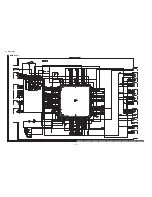

LC
-
46D65E/RU
6 – 4
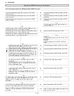
1
2
3
10
9
7
6
5
4
8
J
A
B
C
D
E
F
G
H
I
13
11
19
18
16
15
14
12
17
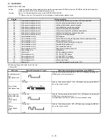
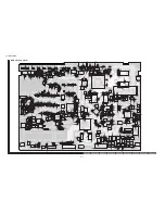
MAIN Unit (Chip Side B)
FL2604
FL2606
C1504
FL2608
C1311
C1506
Q1502
C1312
C1508
Q1505
C1509
C1315
C1316
R600
C1318
FL2610
FL2612
R603
FL2614
R604
FL2615
R605
FL2616
R606
FL2617
R607
R608
R609
C1323
C9601
C1325
C1326
C9603
D1303
C9604
R610
D1304
Q9601
C9605
R611
C1329
D1305
R1301
Q9602
D1306
R612
R1302
C9607
R613
R1303
C1520
C9608
R614
R1304
C9609
R615
R1305
Q9606
R616
R1306
R617
R1307
C4404
Q9608
R618
R1308
C1330
Q9609
R619
C1331
R1309
D1502
C4406
C1332
C4407
D1503
C1527
C1333
C9610
C9611
C4409
R1502
C9612
C9613
R1503
C9614
R620
D1509
D1316
D1317
C9617
D1318
C1530
R1314
R624
R625
C4413
C1533
C4414
D1513
C1538
C1344
D1515
C1345
C1346
C1347
R1320
R630
C9625
R631
R1516
C9626
D9602
C9627
R1517
D9603
R1519
C9629
D9606
R9602
C1543
D9607
R9603
R9604
C1544
D9609
R9605
R9606
R9607
C1547
R9608
C1548
R1520
C1354
C600
R4401
R1521
R9609
C601
R4402
C9632
R4403
C9633
D9610
C9634
R4404
R4405
D9611
C9635
D9612
R4406
R4407
IC9607
R1333
C9638
R4408
R9610
R1334
R9611
C9639
D9615
IC4401
R4409
R1335
R9612
IC4402
D9616
R9613
D9617
R9614
IC4404
D9618
C1360
R9615
IC4405
R9616
IC4407
R9617
R4410
C9640
C1364
IC4409
R4411
C1365
C9642
R4412
C9643
R4413
C1367
C9645
R1535
C7511
C9646
C7512
R1537
R9620
R4418
C9649
R9621
R4419
R9623
R9624
R9625
R9626
R9627
FB2003
C1373
R1540
C9650
R4420
R9628
FB2004
C1374
R1541
R9629
C9651
R4421
FB2005
C5001
R4422
C9652
FB2006
C5002
C9653
FB2007
C5003
C9654
C5004
R4424
FB2008
C5005
C9655
Q5001
FB2009
R1351
C7521
C9656
R4426
C7522
C5006
C5007
R4427
C9657
R1353
C5008
C9658
R9630
R4428
R1354
R9631
C9659
R4429
C7525
C5009
D7502
R1356
D7503
R9633
C7527
R1357
R9634
FB2010
R1358
D7505
R9635
C1381
FB2011
D7506
R9636
C1382
FB2012
C5202
C5203
R9637
FB2013
C1384
R9638
C5204
C9660
FB2014
C5010
D7509
C1385
C9661
R4431
R9639
C5205
C5011
C1386
C5012
R4432
C5206
C1387
R4433
C5013
C5207
R4434
C5014
C5208
C1389
C5209
C5015
R4436
C5016
R4437
C5017
C9667
C5018
R9640
R4438
IC7504
C9668
R9641
C5019
C7535
C9669
C1582
C1583
R9643
C1390
C5210
R9644
R7510
R1368
C1391
C5211
R7511
C5212
R7513
C5213
C5020
C5214
R7514
C9670
R7515
C5021
C5215
C9671
C5216
R7516
C5022
R4443
C5217
R7517
C5023
C5024
C5218
D5001
C5025
C5026
C5027
R9650
C5028
R9651
C5029
R9652
R5002
R9653
R5003
R1378
R5004
R5005
C5221
R5006
C1596
C5222
R5007
C5223
C5030
C5224
R5008
R7524
C1599
C5031
C5225
R4452
C5226
IC5002
R4453
C5033
IC5003
C5227
R4454
C5228
R7528
C5034
C5229
R4455
C8109
C5035
FB5301
C5036
R4456
R4457
C5037
R4458
C5038
R9660
R4459
C8301
C5039
R9661
R5012
R9662
R5013
R9663
R5014
R9664
R5015
C5231
R9665
C5232
R5016
C8306
C5233
C8307
R4460
C5234
C8308
C5040
R4461
C5235
C8309
C5041
R5019
C5236
R4462
C8116
R4463
C8117
R7537
C5043
C5238
C8118
C5044
R7538
C5239
C8119
C5045
R4466
C5046
R4467
C5047
R4468
R5020
C5048
R5021
R4469
C8311
C5049
R5022
C8312
C8313
R5023
C5240
C8120
R5024
R5025
R5026
R5027
R4470
R5028
C5050
R5029
C5051
R4471
C8319
C8125
C5052
C5053
C5054
C5055
D8106
R4476
C5056
C5057
R4477
Q8703
R8103
D8108
R4478
R5030
C8320
R8104
C5058
D8109
R4479
R5031
C8709
C5059
R8105
R5032
R8106
R5033
R8108
R5034
C8324
D8301
R5035
C8325
R8109
R5036
C8326
R5037
R5038
C5060
C8134
C8328
C5061
R8301
C8329
R5039
R7555
C5062
C8712
R8302
C8713
R8303
C5063
C5064
R4484
C8138
R8304
FL504
R7558
C8715
R4485
C5065
R8305
R8111
R7559
C5066
R8306
FL506
C8717
C5067
R8307
R4488
C8718
R8308
C8330
C5068
R8309
C5069
R5042
R8117
R5044
R8118
R5045
C8141
R8119
R5046
C8142
C8336
C8143
C8337
R8310
C8338
C5070
R5048
R5049
R8311
C5071
R8312
C5072
R8313
C8147
C5073
R8314
C5074
R8315
C5075
R8316
C5076
R8317
R8123
C5077
R8318
R8124
C5078
R5051
R8319
R8125
C5079
R8702
R8126
R5052
R8127
C8150
R8128
R5054
C8151
R5055
R5056
R5057
C8153
R8320
R8321
R5059
R8322
C8156
C5082
IC8703
R8323
R8324
C5085
R8131
C5086
R8132
C5087
R8133
R8134
C5088
R5060
FB501
R5061
R8712
R5062
R8713
FB503
R8138
R8139
R5065
R5066
R5067
C5090
R8718
C9104
C8164
C5091
C9105
Q9102
C8166
C8167
C9108
R8140
C8168
C8169
R8143
R5071
R8722
R5072
R8723
C9110
C8170
R8148
C8365
R8149
C9113
FB517
C8173
R8728
C8174
C8175
C8178
R8150
C8179
R8152
R8153
R8730
R8154
R8155
FB1301
R5081
R8156
R5082
FB1303
R5083
C8180
FB1304
R5084
R8159
R5085
C8182
R5086
C8183
R5087
R518
R5088
C8185
R519
FB1309
R5089
C8186
C8187
C8188
R8160
R9101
C8189
R9102
R9103
C1813
R9104
R5090
R520
R5091
R9105
R8165
C1816
R5092
R523
R5093
C8190
R8168
R5094
R9109
C8191
R8169
R5095
C8192
R5096
C8193
R527
R5098
C8194
R528
R1601
C8195
R5099
C8196
C8197
R9110
R8170
C8198
R1605
C8199
R8171
R9112
R8172
R1607
FB1515
R9115
R1609
R8175
R9116
R9117
R8179
R9312
R9313
R9314
R8180
R9121
R9315
R8181
R9122
R9316
R8182
R9317
R9123
R8183
C2003
R9124
R9318
R8184
C2004
C504
R9319
IC1805
R9125
R8185
Q2001
R9126
R8186
C2006
Q2002
R9127
R8187
Q2003
C2007
R9128
Q2004
C2008
R9129
C2009
R9320
R9321
R9322
R9323
R9324
R9130
C2010
R9325
R9131
C2011
C511
R9326
C512
C2012
R9327
R9133
C2013
R9134
R9328
C2014
R9329
R9136
C2016
R9137
C2017
C517
R9138
C2018
R1820
R9139
C2019
C2401
C519
R9330
R9331
C2405
R9332
R9333
R9140
C2020
R9335
R9141
C2021
R9142
R9143
R9337
C2023
R9338
C524
R9339
R561
R9146
R562
C526
R9147
C527
D2004
Q2601
D2005
R9340
R2004
R9341
X5001
FB7501
R9342
X5002
R2007
R2008
R9344
R2009
R570
C2034
R9155
IC2006
C2037
IC2007
R2010
R9159
R2011
C5301
R2012
R2013
C5303
R578
R2014
C5304
C5305
C5306
R2017
Q5303
C5307
R2018
R2019
C5309
R2404
C5310
FB5001
C5311
C5312
FB5002
C5313
FB5003
FB5004
C5314
C5315
FB5005
R2602
R2026
FB5006
FB5007
R2028
R2604
R2029
FB5009
R2606
R2608
R5101
L7501
R5102
R5103
C8200
R2418
R2030
R5104
FB5010
FB5011
C8201
R2419
R2031
R5105
R5106
R2032
FB5012
C8203
R2033
C8204
R2034
R2610
C8205
R2035
C8206
C8207
R2037
D5303
R2420
C8208
C8209
R2421
R2615
C562
R2422
R2423
R2424
R5304
R2618
C565
R2425
D505
R5111
R2619
R2426
R2427
R5307
R2428
C8210
R2040
C568
C8211
C569
R2429
R2041
R5309
C8212
C8213
IC5303
R2620
C8215
R2621
R2045
R2622
C8216
C8217
R2047
R2430
R2048
C570
C8219
R2049
D511
R5311
R5312
C573
R5313
C574
D514
R5314
FB8101
D515
R5315
D516
R5316
R2437
R5317
C8220
FB8104
R5318
FB8105
FB8106
R2052
FB8107
FB8108
R2054
C8226
R2056
R2057
C8228
R5320
C8229
R5321
R5322
R5323
R5324
FB8111
R5325
FB8112
R5326
R5327
R2061
R2063
FB8119
R2067
C590
R2068
C592
R5333
C593
R5334
C594
D535
FB8121
R5335
C595
FB8122
FB8123
C597
FB8124
C598
FB8701
R5339
C599
R2072
R2075
R2078
R5340
R5341
R5342
R5343
R5345
R2082
R2083
C1304
C1308
FL2601
FL2602
Summary of Contents for Aquos LC-42DH77E
Page 50: ...LC 46D65E RU 4 16 M E M O ...
Page 80: ...LC 46D65E RU 7 20 M E M O ...


