background image

LC

-

46D65E/RU

COPYRIGHT © 2008 BY SHARP CORPORATION

ALL RIGHTS RESERVED.

No Part of this publication may be reproduced,
stored in a retrieval system, or transmitted in
any from or by any means, electronic, mechanical,
photocopying, recording, or otherwise, without
prior written permission of the publisher.

SHARP CORPORATION
AV Systems Group
CS Promotion Center
Yaita,Tochigi 329-2193, Japan

Oct. 2008
TQ2617-S  SH. DS

Summary of Contents for Aquos LC-42DH77E

Page 1: ...MENT PROCEDURE 1 ADJUSTMENT PROCEDURE 3 1 CHAPTER 4 TROUBLESHOOTING TABLE 1 TROUBLESHOOTING TABLE 4 1 2 LED flashing specification at the time of the error 4 13 CHAPTER 5 BLOCK DIAGRAM WIRING DIAGRAM 1 MAIN BLOCK DIAGRAM 5 1 2 SYSTEM BLOCK DIAGRAM 5 3 3 OVERALL WIRING DIAGRAM 5 4 CHAPTER 6 PRINTED WIRING BOARD 1 MAIN UNIT PRINTED WIRING BOARD 6 1 2 LED UNIT PRINTED WIRING BOARD 6 5 3 KEY UNIT PRIN...

Page 2: ...tage drop across the resistor All checks must be repeated with the AC cord plug connection reversed If necessary a nonpolarized adaptor plug must be used only for the purpose of completing these checks Any reading of 1 05 V peak this corresponds to 0 7 mA peak AC or more is excessive and indicates a potential shock hazard which must be corrected before returning the monitor to the owner SAFETY NOT...

Page 3: ... lead solder by 40 C and as it has poor solder wettability you may be apt to keep the soldering bit in contact with the PWB for extended period of time However Since the land may be peeled off or the maximum heat resistance temperature of parts may be exceeded remove the bit from the PWB as soon as you confirm the steady soldering condition Lead free solder contains more tin and the end of the sol...

Page 4: ...ment can be returned free of charge to the dealer even if you don t purchase a new product Further collection facilities are listed on the homepage of www swico ch or www sens ch B Information on Disposal for Business Users 1 In the European Union If the product is used for business purposes and you want to discard it Please contact your SHARP dealer who will inform you about the take back of the ...

Page 5: ...AL AUDIO OUTPUT Optical S PDIF Digital audio output C I Common Interface EN50221 R206001 OUTPUT RCA pin AUDIO R L Headphones Ø 3 5 mm jack Audio output OSD language Czech Danish Dutch English Estonian Finnish French German Greek Hungarian Italian Latvian Lithuanian Norwegian Polish Portuguese Russian Slovak Slovene Spanish Swedish Turkish Ukrainian Power Requirement AC 220 240 V 50 Hz Power Consum...

Page 6: ...ct a video setting 1 2 3 4 5 6 7 8 9 10 11 END Exit the MENU screen R G Y B Colour buttons The coloured buttons are correspondingly used to select the coloured items on the screen e g EPG MHEG 5 Teletext INPUT SOURCE Select an input source EPG DTV Display the EPG screen RADIO DTV Switch between Radio and Data mode When only data broadcasting no radio broadcasting is transmitted by DVB the radio br...

Page 7: ...GB terminal COMMON INTERFACE slot EXT8 terminals HDMI3 HDMI terminal USB terminal Headphones AC INPUT terminal 7 8 9 10 11 12 13 14 15 16 WARNING Excessive sound pressure from earphones and headphones can cause hearing loss OPC sensor Remote control sensor OPC indicator Standby On indicator MENU button Power button Volume buttons Programme channel buttons INPUT SOURCE button The HDMI2 and EXT4 ter...

Page 8: ...e 4 short screws into the 4 holes on the rear of the TV 3 1 NOTE To detach the stand unit perform the steps in reverse order Attaching the stand unit Before attaching or detaching the stand unplug the AC cord from the AC INPUT terminal Before performing work spread cushioning over the surface on which you will be laying the TV This will prevent it from being damaged CAUTION Attach the stand in the...

Page 9: ...g the remote control unit for an extended period of time remove the batteries from it When replacing the batteries use alkaline batteries instead of zinc carbon ones Note on disposing batteries The batteries provided contain no harmful materials such as cadmium lead or mercury Regulations concerning used batteries stipulate that batteries may no longer be thrown out with the household rubbish Depo...

Page 10: ...contracts according to changes in temperature This does not affect the TV s performance Cautions regarding use in high and low temperature environments When the TV is used in a low temperature space e g room office the picture may leave trails or appear slightly delayed This is not a malfunction and the TV will recover when the temperature returns to normal Do not leave the TV in a hot or cold loc...

Page 11: ...LC 46D65E RU 1 7 3 DIMENSIONS 1113 0 1023 4 52 0 174 3 106 6 101 4 704 0 756 0 400 0 400 0 295 0 550 0 575 6 429 0 Unit mm ...

Page 12: ...ING OF MAJOR PARTS 1 Removing of Stand Unit and Rear Cabinet 1 Remove the 4 lock screws and detach the Stand Unit 2 Remove the 2 lock screws 3 Remove the 1 lock screw 4 Remove the 4 lock screws 8 lock screws and detach the Rear Cabinet Front Cabinet Rear Cabinet Stand Unit 4 4 2 3 1 ...

Page 13: ...r 2 Disconnect SP Wire Remove the 2 lock screws Detach the Speaker L R 3 Detach the R C LED Unit and disconnect RA Wire 4 Detach the KEY Unit Ass y 5 Detach the KEY Unit from the KEY Button Cover and disconnect KM Wire Speaker Rch Bottom Cover Speaker Lch LED Unit KEY Unit KEY Buttom Cover 2 5 4 3 2 1 2 2 3 2 SP SP RA KM SP RA ...

Page 14: ... RU 2 3 3 Removing of Full Shield and Side AV Cover 1 Remove the 3 lock screws and detach the Side AV Cover 2 Remove the 7 lock screws 4 lock shafts and detach the Full Shield 2 1 2 1 2 Side AV Cover Full Shield ...

Page 15: ...LC 46D65E RU 2 4 4 Removing of Connectors 1 Disconnect all the connectors from all the PWBs 1 LW PL LP 1 LB2 LA 1 1 1 1 MAIN Unit POWER Unit RA SP KM PD LW LP PD 1 LA PL LB1 LB2 1 LB1 ...

Page 16: ... 2 5 5 Removing of MAIN Unit POWER Unit and Power PWB Holder 1 Remove the 8 lock screws and detach the MAIN Unit 2 Remove the 6 lock screws and detach the POWER Unit Ass y 1 2 MAIN Unit POWER Unit POWER Unit Holder ...

Page 17: ...emoving of Panel Support Angles and LCD Panel Module 1 Remove the 16 lock screws and detach the Panel Support Angle 2 Remove the 10lock screws and detach the LCD Panel Module 1 Panel Support Angle 46 LCD Panel Module 2 2 1 ...

Page 18: ...ws Detach the Diffusion Sheet and Diffusion Panel 2 Detach the 4 Sheet Holders 3 Remove the 2 Lamp Holders Detach the Lamp Sockets and Lamps 1 1 1 2 3 Diffusion Sheet Bezel Ass Y Diffusion Plate Sheet Holder Lamp Holder Lamp Socket Lamp BL Chassis Ass y 3 Lamp Holder ...

Page 19: ... OK key to turn the pattern to OFF 2 Entering and exiting the adjustment process mode 1 Unplug the AC power cord of running TV set to force off the power 2 While holding down the VOL and INPUT keys on the set at once plug in the AC power cord to turn on the power The letter K appears on the screen 3 Next hold down the VOL and P keys on the set at once Multiple lines of blue characters appearing on...

Page 20: ... RUSSIA SWEDEN 5 Model name MODEL NAME 6 Item name Max 30 char 7 Parameter Max 60 char 1 Page of present number of total pages 4 Inducing display 3 Present colour system 2 Input that has been selected now 5 Model name 1 16 INPUT1 AUTO EURO 46E_D65 MAIN Version BOOT Version Monitor Version CPLD Version T CON Version H 264 Version EQ DATA CHECKSUM LAMP ERROR MONITOR ERR CAUSE NORMAL STANDBY CAUSE ER...

Page 21: ...green on the upper right 3 16 1 RF AGC ADJ Enter RF AGC auto adjustment execution 2 TUNER ADJ Enter TUNER auto adjustment execution 3 PAL TUNER ADJ Enter PAL TUNER auto adjustment execution 4 RF AGC ADJ CA 8CH Enter RF AGC auto adjustment execution CA 8CH 5 TUNER ADJ CA 8CH Enter TUNER auto adjustment execution CA 8CH 6 PAL TUNER ADJ CA 8CH Enter PAL TUNER auto adjustment execution CA 8CH 7 RF AGC...

Page 22: ...26 4 LCD LUMA DOWN 13 11 16 1 DDRA TEST1 Enter 2 DDRA TEST2 Enter 3 DDRB TEST1 Enter 4 DDRB TEST2 Enter 5 DDRB TEST3 Enter 6 FRC ON OFF Enter 7 SOUSAM DDR BIST Enter 8 SOUSAS DDR BIST Enter 12 16 1 R GAIN LO 0 2 G GAIN LO 0 3 B GAIN LO 0 4 R GAIN HI 0 5 G GAIN HI 0 6 B GAIN HI 0 13 16 1 MONITOR TIME OUT ON 2 MONITOR MAX TEMP 30 3 MONITOR EEP READ WRITE WRITE 4 MONITOR EEP ADR 0x 0 5 MONITOR EEP DA...

Page 23: ...e above phenomenon 1 occurs 5 times consecutively it becomes impossible to turn on the power The power LED remained red 2 Measures 1 Checking with lamp error detection OFF Enter the adjustment process mode referring to 2 Entering and exiting the adjustment process mode If there is a problem with the lamp or lamp circuit the lamp will go out The power LED is green Then you can check the operation t...

Page 24: ...g three digits If the Pass Word is it shifts to the PUBLIC Mode setting screen In another case the screen is erased and it operates in the ordinary mode 2 Exiting the Public Mode screen There are two following ways to exit the Public Mode setting screen 1 Turn off the power 2 Select Execution in the PUBLIC_Mode to execute it Activate the restart under the set content Here the START input SOURCE se...

Page 25: ...d item Decision ok Execution Used by the items Execution and RESET PUBLIC Mode R C Ordinary operation mode It enters the PUBLIC Mode PUBLIC MODE Flag is set to ON PUBLIC Mode It exits the PUBLIC Mode PUBLIC MODE Flag does not change Any set item in PUBLIC Mode is not initialized Public Mode POWER ON FIXED VARIABLE SHUT DOWN MODE NORMAL MAXIMUM VOLUME 60 VOLUME FIXED VARIABLE VOLUME FIXED LEVEL 20 ...

Page 26: ...n Scanning or recording of the digital tuner is enabled disabled when turning off the power It is possible to put into the standby state instantaneously due to power off input Remarks When selecting QUICK the function does not work for the following items The possible method differs from model to model deleting the item selection impossible etc ON TIMER QUICK START DIGITAL FIXED etc Option 0 60 lo...

Page 27: ...process mode inspection mode or hotel mode is enabled regardless of this setting All the keys are enabled regardless of this setting while entering the process mode inspection mode or hotel mode For the main unit s MENU key menu operation is possible regardless of the setting during the initial setting when the power is turned on for the first time Option RESPOND or NO RESPOND loop enabled Default...

Page 28: ...ited When set to NORMAL START MODE FIXED is set to VARIABLE and selection is prohibited Option VARIABLE FIXED AC CTRL or AC RC CTRL loop enabled Default VARIABLE Function When set to FIXED switching to another channel or input is impossible after start up in the set value of INPUT MODE START When set to AC CTRL the unit starts in the set value of INPUT MODE START in the case of the ACON only When ...

Page 29: ...as 232C command RSPW ENABLE POWR0001 is always enabled DISABLE Start up may be impossible at POWR0001 If the 232C command reception module is set to OFF the command is invalid Option OFF or ON loop enabled Default OFF Function The items set in the hotel mode setting menu are enabled or disabled The same item as HOTELMODE in the adjustment process menu Remarks Each operation of the hotel mode is im...

Page 30: ...Full Field Color Bar composite signal Terminal EXT1 SCART IN Feed the PAL full field colour bar signal 75 colour saturation to EXT1 SCART IN 2 Auto adjustment performance Page 4 16 Bring the cursor on PAL ADJ and press OK PAL ADJ OK appears when fin ished Adjustment point Adjustment Conditions Adjustment procedure 1 Setting Signal PAL Split Field Colour Bar RF signal U V Terminal TUNER Feed the PA...

Page 31: ...bar signal 100 colour sat uration to EXT3 COMPONENT IN 2 Auto adjustment performance Page 7 16 Bring the cursor on HDTV ADJ and press OK HDTV ADJ OK appears when finished Adjustment point Adjustment Conditions Adjustment procedure 1 Setting Signal XGA 60Hz 100 Full Field Colour Bar sig nal Terminal EXT4 PC IN Feed the XGA 60Hz 100 full field colour bar signal 100 colour saturation to EXT4 PC IN 2 ...

Page 32: ... for inspection PC mode Modulated light 16 Color temperature High Input signal condition HDMI 1080i 15IRE LO 78IRE HI Adjustment reference device Minolta CA 210 Adjustment procedure CAUTION When the factory settings have been made all user setting data including the channel settings are initialized The adjustments done in the adjustment process mode are not initialized Keep this in mind when initi...

Page 33: ... begins automatically After the set starts the upgrade screen like the figure below is displayed 5 If any of the procedures fails the following upgrade failure screen shows up For the failing procedure the NG marking turns red NOTE In such case try to upgrade the software again If it still fails the hardware may be in trouble SYSTEM UPGRADE System Version E0708021 BANK 1 BANK 2 STATUS UPDATING 30 ...

Page 34: ...ntil the AC power supply is turned off 8 Now the software has been upgraded NOTE Then get the set started and call the process adjustment screen 1 16 to check the main software version CAUTION 1 Do not take out and put in the USB flash memory during formatting 2 It takes about one minute to the rewriting completion Please confirm the upgrade status on the screen becomes 100 3 The AC power supply o...

Page 35: ...ommunication of IC1304 nor mal Pin33 SDA1 Pin34 SCL1 NO Check IC1304 and its peripheral circuits YES Is the audio signal output of pin 13 10 L ch 9 6 R ch of IC1304 POWER_AMP normal NO Check IC1304 and its peripheral circuits YES Is the audio signal output of pins 1 2 L ch 4 3 R ch of P1301 SP terminal normal NO P1301 SP terminal and the peripheral circuit L C filter are checked YES Check Speaker ...

Page 36: ...ting of an external input device that connects with EXT1 Is there a audio input signal in pins 6 IN2L and 2 IN2R of EXT2 SC501 NO Check the setting of an external input device that connects with EXT2 YES EXT1 Is the audio signal input to pins 9 AIN1_L and 10 AIN1_R of IC1302 DSP NO Check the line between SC502 and IC1302 EXT2 Is the audio signal input to pins 13 AIN2_L and 14 AIN2_R of IC1302 DSP ...

Page 37: ...device that connects with HDMI 2 PC Is the audio signal input to pins 19 AIN3_L and 20 AIN3_R of IC1302 DSP NO Check the line between J1301 and IC1302 YES Refer to No sound output in all modes No sound from external input devices 4 Does not the sound of the audio signal input to EXT8 go out Is there a audio input signal in pins 5 IN3L and 4 IN3R of EXT8 J505 NO Check the setting of an external inp...

Page 38: ...utput signal in pins 39 SC1_OUT_L and 38 SC1_OUT_R of IC503 AV_SW YES Check the line between IC503 and SC502 EXT2 Is there a audio output signal in pins 37 SC2_OUT_L and 36 SC2_OUT_R of IC503 AV_SW YES Check the line between IC503 and SC501 NO Check IC503 and its peripheral circuits The audio signal is not output 2 No audio signal output from AUDIO_OUTPUT terminal Is audio signal L R output to pin...

Page 39: ...s No picture on the display 1 The picture doesn t appear in all modes Is the LVDS signal output from IC8101 DIGITAL_AV_DECODER_ _MAIN_CPU_ _VIDEO PROCESSER respectively TA1_P M AC25 AC26 TB1_P M AD25 AD26 TC1_P M AE25 AE26 TD1_P M AE24 AF24 TE1_P M AE23 AF23 TCLK1_P M AF25 AF26 TA2_P M AE22 AF22 TB2_P M AE21 AF21 TC2_P M AE20 AF20 TD2_P M AE18 AF18 TE2_P M AE17 AF17 TCLK2_P M AE19 AF19 YES NO Chec...

Page 40: ...wer supply circuit is checked IC7502 IC9607 IC9604 etc YES Is IF signal sent from pins 16 17 of TUNER TU7501 to pins 40 39 of IC7508 COFDM DEMOD NO Check the tuner IC7508 and their peripheral circuits Replace as required YES Check whether I2C signal normally communicates between TU7501 and IC7508 COFDM DEMOD NO YES Does X7501 20 25MHz oscillate NO Check X7501 and its peripheral circuits YES Is TS ...

Page 41: ... IC503 and IC8101 YES Refer to The picture doesn t appear in all modes External input EXT1 EXT2 No picture on the display 5 Does not the picture of the Y C video signal input to EXT1 go out Does not the picture of the Y C video signal input to EXT2 go out Is Y C video signal sent to pins 20 Y and 15 C of EXT1 SC502 NO Check the setting of an external input device that connects with EXT1 Is Y C vid...

Page 42: ...R of IC8101 DIGITAL AV DECODER MAIN CPU VIDEO PRO CESSER from pins 73 R_TR 75 G_TR 74 B_TR of IC503 NO Check the line between IC503 and IC8101 YES Refer to The picture doesn t appear in all modes External input EXT3 No picture on the display 7 Does not the picture of the component video signal input to EXT3 go out Is a COMPONENT video signal input to pins 3 Y 5 Pb 7 Pr of EXT3 J501 NO Check the se...

Page 43: ...icture doesn t appear in all modes External input EXT8 No picture on the display 9 Does not the picture of the CVBS signal input to EXT8 go out Is a CVBS signal input to pin 6 of EXT8 J505 NO Check the setting of an external input device that connects with EXT8 YES Is CVBS signal from EXT8 J505 sent to pin 12 of IC503 AV_SW NO Check the line between J505 and IC503 YES Is CVBS signal output from pi...

Page 44: ...07 TMDS SW from HDMI 1 SC1502 NO Check the line between HDMI 1 SC1502 and IC1507 YES Is TMDS signal input into pins 39 38 TMDS2_CLK_P N 42 41 TMDS2_D0_P N 45 44 TMDS2_D1_P N 48 47 TMDS2_D2_P N of IC1507 TMDS SW from HDMI 2 SC1501 NO Check the line between HDMI 2 SC1501 and IC1507 Is TMDS signal input into pins 54 53 TMDS3_CLKP N 57 56 TMDS3_D0P N 60 59 TMDS3_D1P N 63 62 TMDS3_D2P N of IC5301 TMDS ...

Page 45: ...R_CVBS signal output from pin 6 of TUNRE TU7501 YES Check the line between TU7501 and IC7503 NO Whether the TUNER circuit operates correctly is checked During external connection No picture on the monitor 2 No picture appears on EXT1 EXT2 connected monitor during the DTV reception Is CVBS signal output into pin 19 of EXT1 SC502 from pin 67 of IC503 AV_SW YES Check the setting of an external input ...

Page 46: ...ine between EXT1 SC502 and IC503 NO Check the setting of an external input device that connects with EXT1 During external connection No picture on the monitor 4 SCART2 No picture from EXT8 appears on EXT2 connected monitor Is CVBS signal output into pin 19 of EXT2 SC501 YES Check the setting of an external input device that connects with EXT2 NO Is CVBS signal output to pin 65 of IC503 YES Check t...

Page 47: ... Red flashes twice Off Red flashes twice Flashes once AC_DET error Flashes twice UR 13 5V error Flashes 3 times D3 3V error Flashes 5 times Panel power supply error Main PWB failure Green flashes once Off Green flashes once Flashes once Initial communication error Communication failure etc Flashes twice Start up confirmation commu nication error Flashes 3 times Regular communication error Flashes ...

Page 48: ... of time acquisition start up 0C Communication error C Ending sequence time out 0D Communication error D Preset start up time out during completion 0E Communication error E Download start up time out 0F Communication error F Time acquisition time out 11 Communication error H Regular communication time out 16 Panel related error Lamp failure 1A Other error 2 Monitor temperature failure 1D Power sup...

Page 49: ...ion the power is turned on again by polling Error type OPC preset LED operation 1 cycle Note Basically debug print logs are analyzed or communication logs are analyzed by a bus monitor Initial communi cation reception failure Flashes once H On Initial communication from the main CPU is not received Request for the monitor model No is not received Communication line failure or main CPU start up fai...

Page 50: ...LC 46D65E RU 4 16 M E M O ...

Page 51: ...LC 46D65E RU 5 1 LC46D65E Service Manual CHAPTER 5 BLOCK DIAGRAM WIRING DIAGRAM 1 MAIN BLOCK DIAGRAM 1 23 10 9 7 6 5 4 8 J A B C D E F G H I 13 11 19 18 16 15 14 12 17 MAIN BLOCK DIAGRAM 1 ...

Page 52: ...LC 46D65E RU 5 2 1 2 3 10 9 7 6 5 4 8 J A B C D E F G H I 13 11 19 18 16 15 14 12 17 MAIN BLOCK DIAGRAM 2 ...

Page 53: ...LC 46D65E RU 5 3 2 SYSTEM BLOCK DIAGRAM 1 2 3 10 9 7 6 5 4 8 J A B C D E F G H I 13 11 19 18 16 15 14 12 17 SYSTEM BLOCK DIAGRAM ...

Page 54: ...LC 46D65E RU 5 4 3 OVERALL WIRING DIAGRAM 1 2 3 10 9 7 6 5 4 8 J A B C D E F G H I 13 11 19 18 16 15 14 12 17 OVERALL WIRING BLOCK DIAGRAM ...

Page 55: ...LC 46D65E RU 6 1 LC46D65E Service Manual CHAPTER 6 PRINTED WIRING BOARD 1 MAIN UNIT PRINTED WIRING BOARD 1 23 10 9 7 6 5 4 8 J A B C D E F G H I 13 11 19 18 16 15 14 12 17 MAIN Unit Side A ...

Page 56: ...509 IC8302 C8332 R7560 R7561 P9101 C8720 FL510 C8721 C8339 FL511 FL512 FL513 R8120 FL516 R8122 P9301 R5053 R8129 C5080 R5058 IC8701 C5081 C5083 IC8704 R8130 C5084 C8159 R8135 C5089 R8136 FB502 R8137 R5063 FB504 R5064 C9101 C8161 X1301 FB505 C8162 FB506 FB507 FB508 R5068 FB509 R5069 C9106 C9107 R8141 R8142 R8144 FB510 R5070 C9301 R8145 R501 FB511 C9302 R502 R8146 FB512 C9303 R503 R5073 FB513 C9304 ...

Page 57: ...LC 46D65E RU 6 3 1 2 3 10 9 7 6 5 4 8 J A B C D E F G H I 13 11 19 18 16 15 14 12 17 MAIN Unit Side B ...

Page 58: ...06 R5033 R8108 R5034 C8324 D8301 R5035 C8325 R8109 R5036 C8326 R5037 R5038 C5060 C8134 C8328 C5061 R8301 C8329 R5039 R7555 C5062 C8712 R8302 C8713 R8303 C5063 C5064 R4484 C8138 R8304 FL504 R7558 C8715 R4485 C5065 R8305 R8111 R7559 C5066 R8306 FL506 C8717 C5067 R8307 R4488 C8718 R8308 C8330 C5068 R8309 C5069 R5042 R8117 R5044 R8118 R5045 C8141 R8119 R5046 C8142 C8336 C8143 C8337 R8310 C8338 C5070 R...

Page 59: ...10 9 7 6 5 4 8 J A B C D E F G H I 13 11 19 18 16 15 14 12 17 LED Unit Side A LED Unit Chip Side A LED Unit Chip Side B LED Unit Side B Q102 Q103 Q104 Q105 R103 R105 R106 R107 R109 R110 R113 R114 R115 R116 R120 C101 C102 C103 C104 D102 D103 D104 IC101 P102 ...

Page 60: ...6 6 3 KEY UNIT PRINTED WIRING BOARD 1 2 3 10 9 7 6 5 4 8 J A B C D E F G H I 13 11 19 18 16 15 14 12 17 KEY Unit Side A KEY Unit Side AChip S155 R153 D152 S154 S152 R151 D151 S151 R152 S153 R154 S156 S157 D155 P151 ...

Page 61: ...are 5 unless otherwise noted K 10 F 1 D 0 5 3 All resistors are 1 16W unless otherwise noted CAPACITOR 1 All capacitors are µF unless otherwise noted P pF µµF 2 All capacitors are 50V unless otherwise noted CAUTION This circuit diagram is original one therefore there may be a slight difference from yours SAFETY NOTES 1 DISCONNECT THE AC PLUG FROM THE AC OUTLET BEFORE REPLACING PARTS 2 SEMICONDUCTO...

Page 62: ...LC 46D65E RU 7 2 2 SCHEMATIC DIAGRAM 1 2 3 10 9 7 6 5 4 8 J A B C D E F G H I 13 11 19 18 16 15 14 12 17 MAIN Unit 1 AND SHADED COMPONENTS SAFETY RELATED PARTS ...

Page 63: ...LC 46D65E RU 7 3 1 2 3 10 9 7 6 5 4 8 J A B C D E F G H I 13 11 19 18 16 15 14 12 17 MAIN Unit 2 ...

Page 64: ...LC 46D65E RU 7 4 1 2 3 10 9 7 6 5 4 8 J A B C D E F G H I 13 11 19 18 16 15 14 12 17 MAIN Unit 3 ...

Page 65: ...LC 46D65E RU 7 5 1 2 3 10 9 7 6 5 4 8 J A B C D E F G H I 13 11 19 18 16 15 14 12 17 MAIN Unit 4 ...

Page 66: ...LC 46D65E RU 7 6 1 2 3 10 9 7 6 5 4 8 J A B C D E F G H I 13 11 19 18 16 15 14 12 17 MAIN Unit 5 ...

Page 67: ...LC 46D65E RU 7 7 1 2 3 10 9 7 6 5 4 8 J A B C D E F G H I 13 11 19 18 16 15 14 12 17 MAIN Unit 6 ...

Page 68: ...LC 46D65E RU 7 8 1 2 3 10 9 7 6 5 4 8 J A B C D E F G H I 13 11 19 18 16 15 14 12 17 MAIN Unit 7 ...

Page 69: ...LC 46D65E RU 7 9 1 2 3 10 9 7 6 5 4 8 J A B C D E F G H I 13 11 19 18 16 15 14 12 17 MAIN Unit 8 ...

Page 70: ...LC 46D65E RU 7 10 1 2 3 10 9 7 6 5 4 8 J A B C D E F G H I 13 11 19 18 16 15 14 12 17 MAIN Unit 9 ...

Page 71: ...LC 46D65E RU 7 11 1 2 3 10 9 7 6 5 4 8 J A B C D E F G H I 13 11 19 18 16 15 14 12 17 MAIN Unit 10 ...

Page 72: ...LC 46D65E RU 7 12 1 2 3 10 9 7 6 5 4 8 J A B C D E F G H I 13 11 19 18 16 15 14 12 17 MAIN Unit 11 ...

Page 73: ...LC 46D65E RU 7 13 1 2 3 10 9 7 6 5 4 8 J A B C D E F G H I 13 11 19 18 16 15 14 12 17 MAIN Unit 12 ...

Page 74: ...LC 46D65E RU 7 14 1 2 3 10 9 7 6 5 4 8 J A B C D E F G H I 13 11 19 18 16 15 14 12 17 MAIN Unit 13 ...

Page 75: ...LC 46D65E RU 7 15 1 2 3 10 9 7 6 5 4 8 J A B C D E F G H I 13 11 19 18 16 15 14 12 17 MAIN Unit 14 ...

Page 76: ...LC 46D65E RU 7 16 1 2 3 10 9 7 6 5 4 8 J A B C D E F G H I 13 11 19 18 16 15 14 12 17 MAIN Unit 15 ...

Page 77: ...LC 46D65E RU 7 17 1 2 3 10 9 7 6 5 4 8 J A B C D E F G H I 13 11 19 18 16 15 14 12 17 MAIN Unit 16 ...

Page 78: ...LC 46D65E RU 7 18 1 2 3 10 9 7 6 5 4 8 J A B C D E F G H I 13 11 19 18 16 15 14 12 17 LED Unit ...

Page 79: ...LC 46D65E RU 7 19 1 2 3 10 9 7 6 5 4 8 J A B C D E F G H I 13 11 19 18 16 15 14 12 17 KEY Unit ...

Page 80: ...LC 46D65E RU 7 20 M E M O ...

Page 81: ...en published to be used for after sales service only The contents are subject to change without notice LC 46D65E RU PartsGuide 1 PRINTED WIRING BOARD ASSEMBLIES 2 LCD PANEL 3 DUNTKE266FM01 KEY Unit 4 DUNTKE685FM05 MAIN Unit 5 DUNTKE687FM05 LED Unit 6 CABINET PARTS 7 LCD MODULE Assembly 8 SUPPLIED ACCESSORIES 9 PACKING PARTS 10 SERVICE JIGS CONTENTS No S08R9LC46D65E LCD COLOUR TELEVISION MODELS LC ...

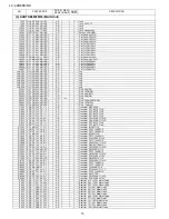
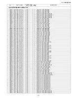
Page 82: ...50V Ceramic C529 VCCCCZ1HH101JY AB J Capacitor 100p 50V Ceramic C530 VCKYCZ1HB221KY AA J Capacitor 220p 50V Ceramic C532 VCKYCZ1HB331KY AA J Capacitor 330p 50V Ceramic C533 VCKYCZ1HB331KY AA J Capacitor 330p 50V Ceramic C534 VCKYCZ1HB331KY AA J Capacitor 330p 50V Ceramic C535 VCKYCZ1HB331KY AA J Capacitor 330p 50V Ceramic C538 VCKYCZ1HB471KY AB J Capacitor 470p 50V Ceramic C539 VCKYCZ1HB471KY AB J...

Page 83: ...J Capacitor 0 1 16V Ceramic C1316 VCKYCY1AB105KY AB J Capacitor 1 10V Ceramic C1317 VCCCCZ1HH180JY AB J Capacitor 18p 50V Ceramic C1318 VCKYCY1AB105KY AB J Capacitor 1 10V Ceramic C1319 RC KZA510WJPZY AB J Capacitor 10 16V Ceramic C1320 VCEASY1CN107MY AC J Capacitor 100 16V Electrolytic C1321 VCKYCZ1HB102KY AB J Capacitor 1000p 50V Ceramic C1322 RC KZA510WJPZY AB J Capacitor 10 16V Ceramic C1323 V...

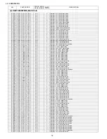
Page 84: ...Ceramic C1582 VCKYCZ1CF104ZY AA J Capacitor 0 1 16V Ceramic C1583 VCKYCZ1HB102KY AB J Capacitor 1000p 50V Ceramic C1596 VCKYCZ1CF104ZY AA J Capacitor 0 1 16V Ceramic C1599 VCKYCZ1HB102KY AB J Capacitor 1000p 50V Ceramic C1801 VCKYCZ1HB222KY AB J Capacitor 2200p 50V Ceramic C1802 RC KZA114WJZZY AB J Capacitor 1 25V Ceramic C1813 RC KZA114WJZZY AB J Capacitor 1 25V Ceramic C1816 RC KZA067WJZZY AB J ...

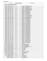
Page 85: ... 027 10V Ceramic C7540 VCKYCZ1EF104ZY AA J Capacitor 0 1 25V Ceramic C7541 VCKYCZ1EF104ZY AA J Capacitor 0 1 25V Ceramic C7542 VCKYCZ1EF104ZY AA J Capacitor 0 1 25V Ceramic C7543 VCCCCZ1HH180JY AB J Capacitor 18p 50V Ceramic C7544 VCCCCZ1HH180JY AB J Capacitor 18p 50V Ceramic C7545 VCEASX1CN107MY AC J Capacitor 100 16V Electrolytic C7546 VCKYCZ1EF104ZY AA J Capacitor 0 1 25V Ceramic C7547 VCKYCZ1E...

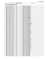
Page 86: ...J107MY AE J Capacitor 100 6 3V Electrolytic C8219 VCKYCZ1CF104ZY AA J Capacitor 0 1 16V Ceramic C8220 VCKYCZ1CF104ZY AA J Capacitor 0 1 16V Ceramic C8301 VCKYCZ1EB103KY AA J Capacitor 0 01 25V Ceramic C8303 RC KZA195WJZZY AB J Capacitor 10 10V Ceramic C8306 VCKYCZ1CF104ZY AA J Capacitor 0 1 16V Ceramic C8307 VCKYCZ1CF104ZY AA J Capacitor 0 1 16V Ceramic C8308 VCKYCZ1CF104ZY AA J Capacitor 0 1 16V ...

Page 87: ...1 25V Ceramic C9667 VCKYCZ1CB223KY AC J Capacitor 0 022 16V Ceramic C9668 VCKYCZ1EB682KY AB J Capacitor 6800p 25V Ceramic C9669 VCKYCZ1EB682KY AB J Capacitor 6800p 25V Ceramic C9670 RC KZA195WJZZY AB J Capacitor 10 10V Ceramic C9672 VCAAPE0JJ227MY AE J Capacitor 220 6 3V Electrolytic D501 VHPGPFSV51V 1 AG N J Diode GPFSV51V D502 RH EXA520WJZZY AB J Zener Diode MAZ8051GML D503 RH EXA520WJZZY AB J Z...

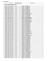
Page 88: ...B J Balun BLN 0077TA FB515 RBLN 0077TAZZY AB J Balun BLN 0077TA FB516 RBLN 0077TAZZY AB J Balun BLN 0077TA FB517 RBLN A188WJZZY AA J Balun BLN A188WJ FB518 RBLN 0077TAZZY AB J Balun BLN 0077TA FB519 RBLN 0077TAZZY AB J Balun BLN 0077TA FB520 RBLN A188WJZZY AA J Balun BLN A188WJ FB1301 RBLN A188WJZZY AA J Balun BLN A188WJ FB1302 RBLN A188WJZZY AA J Balun BLN A188WJ FB1303 RBLN A188WJZZY AA J Balun ...

Page 89: ...333W 1Y AQ N J IC STA333W13TR IC1305 VHINJM3414V 1Y AF J IC NJM3414AV TE1 IC1503 RH iXC697WJQZS AH J IC EDID PC IC1504 RH iXC442WJN1S AK N J IC EDID HDMI IC1507 VHIBU16028K 1Q AP N J IC BU16028KV IC1805 VHIBH33FB1G 1Y AD J IC BH33FB1WG TR IC2001 VHITCVHC32T 1Y AE J IC TC74VHC32FT EL IC2002 VHIS80927NM 1Y AC J IC S 80927CNMC G8XT2G IC2003 RH IXC331WJQZQ AQ J IC R5F364V6NFB U0 IC2004 VHITC7SH00U 1Y ...

Page 90: ... J Transistor 2SA1530A T112 1R Q512 VSDTC314TK 1Y AC J Transistor DTC314TKT146 Q513 VSDTC314TK 1Y AC J Transistor DTC314TKT146 Q1301 VSIMH23T110 1Y AC J Transistor IMH23T110 Q1504 VSRDTC144EE 1Y AA J Transistor PDTC144EE 115 Q1506 VSRDTC144EE 1Y AA J Transistor PDTC144EE 115 Q1516 VSIMD2A 1Y AC J Transistor IMD2AT108 Q1802 VSRDTC144EE 1Y AA J Transistor PDTC144EE 115 Q1803 VSDTA124EKA 1Y AB J Tran...

Page 91: ...e R568 VRS CY1JF000JY AA J Resistor 0 1 16W Metal Oxide R569 VRS CZ1JF101JY AA J Resistor 100 1 16W Metal Oxide R570 VRS CZ1JF103JY AA J Resistor 10k 1 16W Metal Oxide R571 VRS TQ2EF750JY AA J Resistor 75 1 4W Metal Oxide R572 VRS TQ2EF750JY AA J Resistor 75 1 4W Metal Oxide R573 VRS CZ1JF101JY AA J Resistor 100 1 16W Metal Oxide R574 VRS CZ1JF102JY AA J Resistor 1k 1 16W Metal Oxide R575 VRS CZ1J...

Page 92: ... Metal Composition R1359 VRS TV1JD000JY AA J Resistor 0 1 10W Metal Oxide R1360 VRS TV1JD000JY AA J Resistor 0 1 10W Metal Oxide R1361 VRS TV1JD000JY AA J Resistor 0 1 10W Metal Oxide R1362 VRS TV1JD000JY AA J Resistor 0 1 10W Metal Oxide R1363 VRS CY1JF102JY AA J Resistor 1k 1 16W Metal Oxide R1364 VRS TW2ED101JY AA J Resistor 100 1 4W Metal Oxide R1365 VRS CY1JF104JY AA J Resistor 100k 1 16W Met...

Page 93: ...1JF103JY AA J Resistor 10k 1 16W Metal Oxide R2048 VRS CZ1JF103JY AA J Resistor 10k 1 16W Metal Oxide R2049 VRS CZ1JF100JY AA J Resistor 10 1 16W Metal Oxide R2050 VRS CZ1JF100JY AA J Resistor 10 1 16W Metal Oxide R2051 VRK SA1JF100JY AB J Resistor 10 1 16W Metal Composition R2052 VRS CZ1JF223JY AA J Resistor 22k 1 16W Metal Oxide R2054 VRS CZ1JF223JY AA J Resistor 22k 1 16W Metal Oxide R2056 VRS ...

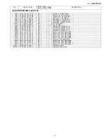
Page 94: ...JF103JY AA J Resistor 10k 1 16W Metal Oxide R5308 VRK SA1JF100JY AB J Resistor 10 1 16W Metal Composition R5309 VRS CZ1JF562FY AA J Resistor 5 6k 1 16W Metal Oxide R5313 VRS CZ1JF273FY AA J Resistor 27k 1 16W Metal Oxide R5344 VRK SA1JF100JY AB J Resistor 10 1 16W Metal Composition R5345 VRK SA1JF472JY AA J Resistor 4 7k 1 16W Metal Composition R7508 VRS CZ1JF000JY AA J Resistor 0 1 16W Metal Oxid...

Page 95: ...6W Metal Oxide R8313 VRS CZ1JF000JY AA J Resistor 0 1 16W Metal Oxide R8314 VRK SB1FF000JY AA J Resistor 0 1 32W Metal Composition R8315 VRK SB1FF000JY AA J Resistor 0 1 32W Metal Composition R8316 VRS CZ1JF000JY AA J Resistor 0 1 16W Metal Oxide R8317 VRS CZ1JF000JY AA J Resistor 0 1 16W Metal Oxide R8318 VRS CZ1JF000JY AA J Resistor 0 1 16W Metal Oxide R8319 VRK SB1FF000JY AA J Resistor 0 1 32W ...

Page 96: ... 1 16W Metal Oxide R9630 VRS CZ1JF101JY AA J Resistor 100 1 16W Metal Oxide R9632 VRS CZ1JF332JY AA J Resistor 3 3k 1 16W Metal Oxide R9634 VRS CZ1JF123FY AA J Resistor 12k 1 16W Metal Oxide R9635 VRS CZ1JF163FY AB J Resistor 16k 1 16W Metal Oxide R9637 VRS CZ1JF103JY AA J Resistor 10k 1 16W Metal Oxide R9638 VRS CZ1JF101JY AA J Resistor 100 1 16W Metal Oxide R9639 VRS CZ1JF101JY AA J Resistor 100...

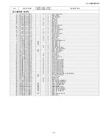
Page 97: ...03 VS2SC3928AR 1Y AB J Transistor 2SC3928A T112 1R Q104 VS2SC3928AR 1Y AB J Transistor 2SC3928A T112 1R Q105 VS2SC3928AR 1Y AB J Transistor 2SC3928A T112 1R R103 VRS CY1JF161JY AA J Resistor 160 1 16W Metal Oxide R105 VRS CJ1JF103JY AA J Resistor 10k 1 16W Metal Oxide R106 VRS CY1JF223JY AA J Resistor 22k 1 16W Metal Oxide R107 VRS CY1JF393JY AA J Resistor 39k 1 16W Metal Oxide R110 VRS CY1JF103JY...

Page 98: ...ARTS 1 1 1 1 3 1 4 1 2 1 7 36 6 29 35 34 37 38 46 12 5 43 41 2 47 2 1 3 1 3 2 13 48 19 3 20 45 15 40 15 40 45 39 45 44 44 16 44 18 10 8 8 10 16 42 14 14 27 24 26 34 32 33 30 28 25 2 2 7 45 4 4 1 4 2 23 11 45 31 33 1 6 1 6 1 5 1 5 ...

Page 99: ...JFN AC J Screw x4 D Sub 16 PCUSGA079WJZZ S Corner Lug x8 17 PCUSGA099WJZZ N S Corner Lug 18 PMLT A578WJZZ N S 10 1 0 185 RT 19 PSHEPA543WJZZ S Diffusion Sheet x2 20 PSLDMB480WJFW N S Full Shield 23 QCNW H324WJQZ N S Connecting Cord KM 24 QCNW H328WJQZ N S Connecting Cord RA 25 QCNW H339WJQZ N S Connecting Cord LA 26 QCNW H336WJQZ N S Connecting Cord PD 27 QCNW H332WJQZ N S Connecting Cord LB 28 QC...

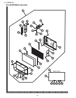
Page 100: ...LC 46D65E RU 20 7 LCD MODULE Assembly 1 3 9 16 5 15 11 14 10 22 19 20 18 6 8 25 12 24 6 7 2 3 17 21 13 23 27 28 25 2 4 26 28 28 27 27 27 28 ...

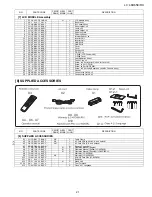
Page 101: ...CORFA061WJZZ J Ferrite Core x4 22 XHPS830P06WS0 J Screw x10 for Inverter Unit x4 for Cover x6 23 LX HZA045WJF7 J Screw x4 for C PWB 24 LX HZA046WJF7 J Screw x4 for GND PWB 25 LX EZA028WJF9 J Screw x16 for fixing Bezel Ass y and BL Chassis Ass y 26 PMLT A579WJZZ J Gasket 27 QEARZA148WJZZ J Conductivity Cloth A x2 28 QEARZA149WJZZ J Conductivity Cloth B x2 8 SUPPLIED ACCESSORIES X1 LHLDWA173WJKZ AE ...

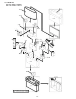
Page 102: ...LC 46D65E RU 22 9 PACKING PARTS 㵘 Not Replacement item S5 S1 S8 S8 S3 S12 S8 S11 S4 S6 S7 S2 S8 S9 S13 S10 S12 ...

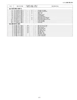
Page 103: ...ZZ N Buffer Material Top Center S10 SPAKXC151WJZZ N Buffer Material Bottom Center S11 SSAKAA009WJZZ Polyethylene Bag S12 SSAKAA111WJZZ Polyethylene Bag S13 TLABM5584BMZZ Case Label 10 SERVICE JIGS N QCNW G616WJQZ BK J Main LCD Control LW N QCNW H347WJQZ AY J Main LCD Control LP N QCNW H348WJQZ AW J MAIN LED RA N QCNW H185WJQZ AV J MAIN POWER LB N QCNW H184WJQZ AX J Main Power PD N QCNW G445WJQZ AP...

Page 104: ... be reproduced stored in a retrieval system or transmitted in any from or by any means electronic mechanical photocopying recording or otherwise without prior written permission of the publisher SHARP CORPORATION AV Systems Group CS Promotion Center Yaita Tochigi 329 2193 Japan Oct 2008 TQ2617 S SH DS ...

Reviews: