

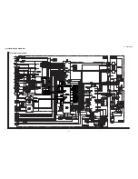
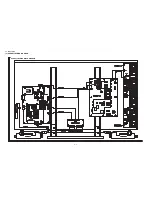
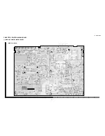
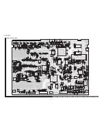


LC
-
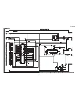
46D65E/RU
6 – 2
1
2
3
10
9
7
6
5
4
8
J
A
B
C
D
E
F
G
H
I
13
11
19
18
16
15
14
12
17
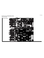
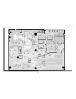
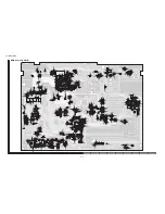
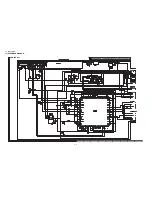
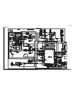
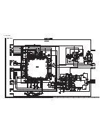
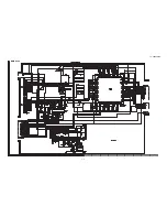
MAIN Unit (
Chip Side A
)
C1501
FL2605
C1502
FL2607
C1310
FL2609
C1313
C1507
Q1504
C1314
Q1506
C1317
X9301
C1319
R601
FL2611
R602
C1320
C1321
C1322
C1324
D1301
Q1516
C9602
D1302
C1327
C1328
C9606
D1307
Q9603
Q9604
D1308
Q9605
D1309
Q9607
Q4401
C4405
LUG501
D1501
IC1301
IC1302
LUG502
IC1303
LUG503
C4408
D1504
C1334
D1310
IC1304
LUG504
R1501
D1311
LUG505
C1335
IC1305
D1506
IC1306
LUG506
D1312
C1336
D1507
C1337
D1313
LUG507
LUG508
R1504
D1508
R1310
C1338
D1314
D1315
LUG509
R1311
R1505
C9615
R621
C1339
C9616
R1506
R622
R1507
R623
R1508
C4410
C9618
C4411
C9619
R1509
IC1501
IC1502
R1316
R626
R1317
IC1503
R627
LUG510
R1318
IC1504
C1340
R628
LUG511
C4415
R1319
C1341
R629
C4416
D1512
C1342
IC1507
C1343
R1510
C9620
C9621
R1511
C9622
R1512
R1513
C9623
C9624
C1348
R1321
D1519
D9601
C1349
R632
R1322
R633
C4420
C9628
D9604
C1540
R1324
R9601
C4421
SC9301
D9605
R1326
R1327
D9608
R1328
C1350
D1521
R1329
C1351
D1522
C1352
D1523
C1353
C9630
C9631
IC9601
X2001
C1355
P5001
P5002
IC9602
R1522
C1356
R1523
IC9603
C1357
IC9604
R1330
C1358
IC9605
C1359
R1331
C7501
C9636
IC9606
R1332
C7502
C9637
R1527
D9613
C7503
IC9608
D9614
C7504
IC9609
Q7501
C7505
C1552
R1336
C7506
C1553
IC4403
R1337
Q7503
C7507
C1554
Q7504
C7508
C1361
R1339
C7509
Q7505
D9619
IC4406
C1362
C1363
R9618
IC4408
IC9610
C9641
R9619
C611
C612
C1366
C613
R4414
C9644
C614
C1368
R1340
C7510
D9620
C615
R4415
C1369
R1341
R4416
R1342
C7513
C9647
R1343
R4417
C7514
C9648
R1344
C7515
R9622
R1346
C7516
R1347
C7517
C1370
C7518
FB2001
R1349
C1371
FB2002
C1372
C1375
C1376
C1377
R4423
R1350
C1378
C7520
R4425
C1379
R1352
Q5002
R1548
C7524
R1549
R1355
D7501
VA8101
R9632
C7526
VA8102
D7504
C1380
C7528
C5201
P8101
R1359
R7501
C7529
P8102
R7502
D7507
P8103
C1383
R7503
D7508
R4430
R1550
R7504
R7505
C9662
R1552
R7506
C9663
R1553
R7507
R7508
C1388
R1554
R1360
C7530
C9664
R7509
R4435
R1361
IC7501
C7531
C9665
R1362
FB2402
C7532
IC7502
C9666
C7533
IC7503
FB2403
R1363
D7510
FB2404
C7534
R1364
D7511
R1365
R9642
R1366
C7536
R1367
C7537
C7538
IC7508
R9645
C7539
R7512
R9646
R9647
R9648
R4441
R9649
R4442
R1562
C9672
R1563
R1370
C7540
R7518
R1565
R1371
R7519
C7541
C5219
R4446
R1566
R1372
C7542
R4447
R1567
R1373
C7543
R1568
R1374
C7544
FL1501
R5001
R1569
R1375
C7545
FL1502
C7546
FL1503
R1377
C7547
R9654
R7520
C7548
C5220
R9655
C8101
C7549
R7521
R9656
C8102
R7522
R9657
C8103
R7523
R9658
R1570
C8104
R9659
R5009
R1571
C8105
IC5001
R7525
R1572
C8106
R7526
C8107
R7527
C8108
C7550
R7529
C7551
C7552
R5203
C7553
R5204
R5010
C7554
R5205
Q501
R5011
SC2601
R5206
Q502
C8303
Q503
R5207
C5230
C8110
Q504
R5208
R7530
IC5201
R5209
Q505
R7531
R7532
IC5202
R5017
R7533
IC5203
R5018
IC5204
C8114
R7534
C8115
R7535
R7536
C5237
R4464
R5210
R4465
R5211
R5212
R5213
Q510
R5214
Q511
R5215
R5216
Q512
Q513
R5219
L501
C8121
C8315
SC5301
SC5302
L502
R7542
L503
R7544
C8701
D8101
R7545
R4472
C8702
C8126
D8102
R7546
R1593
R4473
C8703
D8103
R7547
D8104
R1594
R4474
R5220
R7548
D8105
R4475
R8101
R7549
R5221
R5222
R8102
D8107
R5223
R5224
R5225
C8321
R5226
L2613
R5227
R8107
L2614
R5228
R7550
L2615
R5229
IC8101
R7551
L2616
IC8102
R7552
L2617
IC8103
R7553
L2618
R4480
R4481
FL501
R4482
FL502
R4483
FL503
R7557
R5230
R5231
FL505
R4486
R5232
R8112
R4487
FL507
R5040
FL508
R5041
C8719
IC8301
FL509
IC8302
C8332
R7560
R7561
P9101
C8720
FL510
C8721
C8339
FL511
FL512
FL513
R8120
FL516
R8122
P9301
R5053
R8129
C5080
R5058
IC8701
C5081
C5083
IC8704
R8130
C5084
C8159
R8135
C5089
R8136
FB502
R8137
R5063
FB504
R5064
C9101
C8161
X1301
FB505
C8162
FB506
FB507
FB508
R5068
FB509
R5069
C9106
C9107
R8141
R8142
R8144
FB510
R5070
C9301
R8145
R501
FB511
C9302
R502
R8146
FB512
C9303
R503
R5073
FB513
C9304
R504
R5074
FB514
R505
FB515
R5075
C9112
R506
R5076
FB516
R507
R5077
R508
FB518
R5078
R8729
R509
FB519
C1801
R8151
C1802
R510
FB520
R8731
R511
Q1802
R8732
FB1302
R512
R8733
Q1803
R513
R8734
R514
FB1305
R515
FB1306
R516
R517
FB1307
C8184
Q1808
FB1308
D9101
Q1809
D9102
FB1501
P2001
FB1502
R8162
P2002
FB1503
P2003
FB1504
P2004
FB1310
LUG1501
R521
FB1311
LUG1502
R9106
R522
LUG1503
R9107
R8167
R9108
R524
IC9101
R525
R526
IC9104
R9301
R529
R9302
R9303
R9304
R1604
R9111
R9305
R9306
R9307
R9113
R9114
R9308
R530
IC9301
R9309
R531
D1802
IC9302
R532
R533
R534
SC1501
FB9601
R9119
R1801
P2401
R535
SC1502
FB9602
R536
P2402
FB9603
R537
R9310
FB9604
R538
R9311
R539
L1301
FB9605
L1302
FB9606
L1303
R9120
L1304
C501
C2001
L1305
FB4402
C502
C2002
L1306
FB4403
C503
R540
C2005
C505
R541
R542
C506
P2603
C507
R543
R8188
R544
C508
R8189
C509
R545
R546
R547
R548
R549
R1622
R1817
C510
R1819
X7501
R9132
C513
C514
R550
R9135
C2015
R551
C515
VA5301
R552
C516
VA5302
R553
VA5303
C518
R554
VA5304
SC4401
R555
VA5305
R556
C2402
VA5306
R557
VA5307
C2403
R558
C2404
VA5308
VA5309
Q2401
Q2402
C2406
C2407
R9334
C520
C2408
L9601
C521
Q2405
R9336
L9602
C2022
C522
L9603
C523
Q2407
L9604
VA5310
C2024
L9605
C2601
VA5311
C525
C2025
VA5312
C2026
D2002
L9606
C2602
VA5313
C2027
D2003
R563
C2603
L9607
R9148
VA5314
R564
C528
C2028
C2410
C2605
VA5315
R565
C529
C2029
R2001
D2006
C2606
VA5316
R566
R2002
C2607
R2003
R567
C2608
R568
R569
R2005
R2006
R9343
R9150
C2030
C530
R9151
C531
IC2001
C2031
C532
C2032
IC2002
R9153
C2033
IC2003
C533
IC2004
C534
IC2005
C535
C2035
R571
C2036
R572
C537
R573
R9158
C538
R574
C539
R575
C5302
R576
R577
R2015
R579
D2401
Q5301
Q5302
R2016
D2402
D2403
C540
C5308
D2404
TH2001
R2401
C541
D2405
C542
R2402
R2403
C543
C544
R580
C545
R2405
R581
R582
R2406
C546
R583
R2407
C547
R584
R2408
R2020
C548
R2021
C549
IC2401
R2409
R585
IC2402
R2022
R586
R2023
IC2403
R587
R588
R2024
R2601
R2025
R589
S2001
S2002
R2603
R2027
C5317
S2003
C550
R2410
S2004
C551
S2005
R2605
C552
S2006
C553
S2007
R2607
R590
C554
R5100
IC2601
C555
R591
R2609
IC2602
C556
R592
C557
R593
R2417
R594
C558
R595
C559
X8102
R596
R597
R5107
R598
R5108
L7508
R2611
R599
R2612
D5302
R2613
C560
R2614
C561
R2039
R5301
D502
R5302
R2616
R2617
C563
D503
R5303
D504
C564
R5305
C566
D506
R5306
R5112
C567
D507
R5113
D508
R5308
D509
IC5301
R2042
IC5302
C8214
R2044
C8218
D510
R5310
C571
C572
D512
D513
R2433
C575
R2435
C576
C577
D517
FB8103
R2050
D518
R2438
C578
C8221
D519
R2051
R2439
C579
C8222
C8223
C8224
C8225
R2055
X8702
C8227
R2058
D520
R2440
C580
IC501
R2059
D521
R2441
C581
IC502
D522
C582
R2442
IC503
D523
C583
R2443
D524
FB8110
C584
R2444
IC504
D525
C585
R2445
C586
R2446
D527
C587
R2447
R2060
C588
R2448
R5328
R5329
C589
R2062
R2064
R2065
P1301
R2066
R5330
D531
R2069
FL2001
R5331
C591
D532
R5332
D533
D534
VA1501
VA1502
R5336
C596
VA1503
R5337
VA1504
R2070
R5338
VA1505
R2071
VA1506
FB8702
FB8126
VA1507
R2073
VA1508
R2074
VA1509
R2076
L8103
R2077
R2079
VA1510
R5344
VA1511
VA1512
R5346
VA1513
R5347
VA1514
R5348
R2080
VA1515
R5349
R2081
VA1516
C1301
C1302
C1303
R5350
P9601
C1305
Q1301
Q1302
C1306
P9602
C1307
P9603
C1309
FL2603
Summary of Contents for Aquos LC-42DH77E
Page 50: ...LC 46D65E RU 4 16 M E M O ...
Page 80: ...LC 46D65E RU 7 20 M E M O ...