background image

Saia-Burgess Controls AG

Manual 

Manual PCD 1 / PCD 2 Series


│ Document 26


/

 737 E

N22 │ 2013-11-26

4

Communication interfaces

4-20

Serial interfaces on socket A

4.6.6  MP-Bus with PCD7.F180, Port #1 (without PCD1.M110)

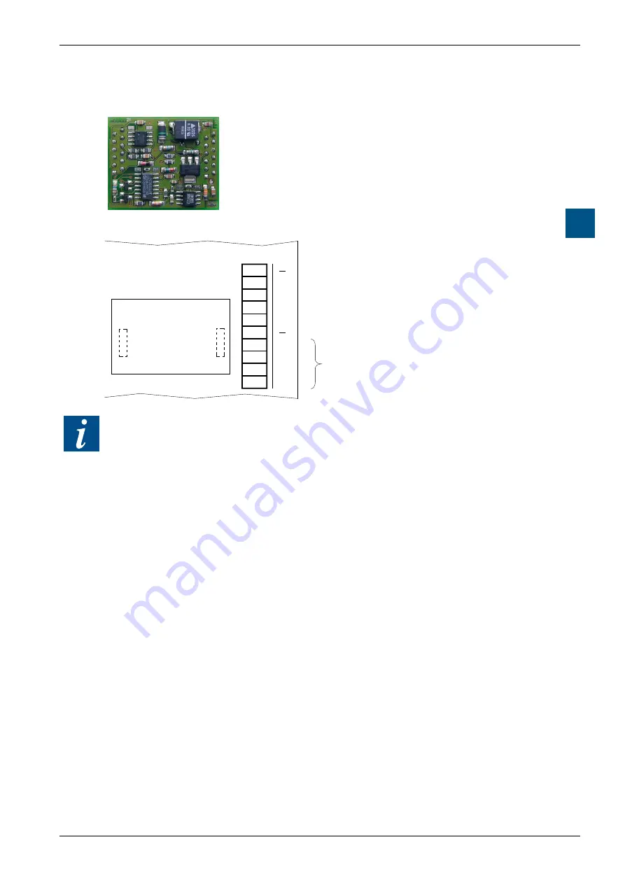
PCD7.F180: 

Connecting module for MP-Bus, for socket A

The user has a facility to connect an MP-Bus line with 8 drives 

and sensors.

Connections

10 
11 
12 
13 
14 
15 
16 
17 
18 
19 

19 

18 

17 

16 

14 

13 

12 

11 

PCD7.F180 

MP
,MFT’
,IN’ 
GND 

Socket A

Screw terminal block, socket A

MP-Bus signal line (18 V in/out)
MFT programming unit (MP-Bus internal)

MFT programming unit detection (input 10 kΩ, Z5V1)

Earth connection, MFT programming unit

GND 

GND

Not used

There are the following parameterization devices of BELIMO

®

Manual Control Unit 

MFT-H 

With its own power supply/batteries

PC-Tool  

MFT-P 

With the adapter ZIP-RS-232

Summary of Contents for PCD1 Series

Page 1: ...Document 26 737 Edition EN22 2013 11 26 Manual PCD1 PCD2 Series ...

Page 2: ...for the Saia PCD Classic family 3 6 3 4 CPU overview 3 7 3 4 1 PCD1 M1xx 3 7 3 4 2 Block diagram PCD1 M1xx 3 8 3 4 3 Hardware and firmware versions for the PCD1 3 9 3 4 4 Firmware Upgrade for the PCD1 M110 PCD1 M120 and PCD1 M130 3 10 3 4 5 Firmware Upgrade for the PCD1 M125 and PCD1 M135 3 10 3 4 6 PCD2 M1x0 M480 Hardware and Firmware 3 11 3 4 7 Block diagram PCD2 Mxx0 3 14 3 4 8 Hardware and fir...

Page 3: ...y 3 45 3 16 Data storage in case of power outage 3 46 3 17 Backup of the user program flash card for PCD2 M170 M480 3 47 3 17 1 General 3 47 3 17 2 Copying the application to the flash card backup 3 48 3 17 4 Backup restore of RAM texts DBs at run time 3 50 3 18 Hardware clock Real Time Clock 3 55 3 18 1 Clock module PCD2 F500 obsolete PCD2 M110 M120 only 3 55 3 19 Monitoring the CPU watchdog 3 56...

Page 4: ... 5 RS 485 communiaction interface PORT 6 only on PCD2 M480 4 10 4 5 6 USB interface as PGU interface on PCD2 M480 4 11 4 5 7 Profi S Net on PCD2 M480 4 12 4 6 Plug in interfaces modules Socket A 4 13 4 6 1 RS 485 422 with PCD7 F110 Port 1 with PCD1 M110 hard wired 4 13 4 6 2 RS 232 with PCD7 F120 suitable for modem Port 1 without PCD1 M110 4 15 4 6 3 RS 232 with PCD7 F121 Port 1 without PCD1 M110 ...

Page 5: ...lectrically isolated 5 19 5 4 Digital output modules 5 21 5 4 1 PCD2 A300 6 digital outputs for 2 A each 5 22 5 4 2 PCD2 A400 8 digital outputs for 0 5 A each 5 24 5 4 3 PCD2 A460 16 digital outputs for 0 5 A each with ribbon connector 5 26 5 4 4 PCD2 A465 16 digital outputs for 0 5 A each 5 29 5 5 Digital output modules electrically isolated 5 31 5 5 1 PCD2 A200 4 relays with make contacts with c...

Page 6: ...e weighing modules 5 104 5 15 Analogue thermocouple modules 5 105 5 16 Fast counting modules 5 106 5 16 1 PCD2 H100 counting module up to 20 kHz 5 107 5 16 2 PCD2 H110 general purpose counting measuring module up to 100 kHz 5 112 5 17 SSI interface modules 5 114 5 17 1 PCD2 H150 SSI interface module for absolute encoder 5 115 5 18 Motion control modules for stepper motors 5 118 5 18 1 PCD2 H210 Mo...

Page 7: ...ols supported by the firmware A 5 A 3 2 Protocols implemented in the user program A 5 A 4 Installation direction and relays contact protection A 6 A 4 1 Installation direction for switching low voltages A 6 A 4 2 Installation direction for switching higher voltages A 6 A 4 3 Switching inductive loads A 8 A 4 4 Relay manufacturer s information on RC unit dimensioning A 8 A 5 Order codes A 10 ...

Page 8: ...TIP by PCD2 W2x0 wrong polarity on input description of the Jumper positions for PCD2 K525 calculation of the spark deletion in the appendix EN15 2008 07 22 Chapt 5 Chapt 5 Added new module PCD2 W525 Definition of input signals revised EN16 2008 12 17 Chapt 3 4 Chapt 5 7 Chapt 5 12 1 Chapt 6 Chapt 7 1 PCD2 M150 now with FW update Wiring PCD2 W2x0 corrected Digital analog values PCD2 W2x0 correc te...

Page 9: ...Brands and trademarks Content 0 8 0 0 2 Brands and trademarks Saia PCD and Saia PG5 are registered trademarks of Saia Burgess Controls AG Technical modifications are based on the current state of the art technology Saia Burgess Controls AG 2003 All rights reserved Published in Switzerland ...

Page 10: ...phical index The graphical index singles out some highlights from the Hardware manual for the PCD1 PCD2 Series and allows you to click on a component connector to jump straight to the corresponding section The facility to jump to any section from the table of contents is still to be completed 1 1 PCD1 M110 M120 M130 M125 M135 ...

Page 11: ...Saia Burgess Controls AG Manual Manual PCD1 PCD2 Series Document 26 737 EN22 2013 11 26 PCD2 M110 M120 M150 Graphical index 1 2 1 1 2 PCD2 M110 M120 M150 ...

Page 12: ...Saia Burgess Controls AG Manual Manual PCD1 PCD2 Series Document 26 737 EN22 2013 11 26 PCD2 M170 Graphical index 1 3 1 1 3 PCD2 M170 ...

Page 13: ...Saia Burgess Controls AG Manual Manual PCD1 PCD2 Series Document 26 737 EN22 2013 11 26 PCD2 M480 Graphical index 1 4 1 1 4 PCD2 M480 ...

Page 14: ...ld bus such as Profibus LIOs Local I Os these are connected to the CPU via the I O bus or a RIO i e with the shortest possible cables Modules Input output elements mounted in a housing matched to the PCD1 2 system Module holders CPUs RIOs or LIOs to which modules may be attached The aim of the Overview section is to present the essentials of planning and installing control systems with PCD1 2 comp...

Page 15: ... PCD1 4 4 64 64 PCD2 M120 150 8 8 8 16 128 128 1 256 1 PCD2 M170 8 8 24 32 128 384 2 512 2 PCD2 M480 8 8 56 64 128 896 1 1024 1 PCD2 modules and PCD3 modules with 16 I Os each The values in brackets have to be subtracted from the maximum number of digital I Os because of the watchdog relay If you want to expand PCD2 CPUs with PCD3 LIOs RIOs please refer to the planning instructions in the PCD3 man...

Page 16: ...be In extreme cases switch to PCD3 expansion units Estimate consumption from the 24 V supply Use estimated values from the section on Hardware These estimated values can be found in section 3 8 5 Power consumption of PCD2 PCD3 input output modules Note that in most applications the outputs place the heaviest load on the 24 V sup ply For 16 outputs with a load current of 0 5 A each the loading will...

Page 17: ...wire by the shortest route The shield is generally connected to one side of the switching cabinet only unless there is a potential equalization with significantly lower resistance than the shield resistance Inductivities installed in the same switching cabinet e g contactor coils should be provided with suitable suppressors RC elements Switching cabinet components with high field intensity e g tra...

Page 18: ...intuitively by anyone the standard tool for comissioning service support and visualization of machines units and installations The user can retrieve pre defined device and system specific HTML pages giving access to all data on controllers and RIOs Graphical elements images diagrams etc as well as text documents operating and repair manuals can also be integrated into the HTML pages to provide a p...

Page 19: ...nter and motion control modules are used as these may con sume a lot of power Atmospheric conditions Ambient temperature Mounting on vertical surface with vertically aligned connection terminals 0 55 C In all other mounting positions a reduced temperature range of 0 40 C applies Storage temperature 25 85 C Relative humidity 30 95 without condensation Vibration resistance Vibration according to EN ...

Page 20: ...35 2 x 35 mm Connections Screw terminals Unless specified otherwise for wires of 1 5 mm2 AWG 16 or 2 x 0 5 mm2 2 x AWG 20 Plug in screw terminals The terminal block may only be plugged onto 20 times It must then be replaced to guarantee a reliable contact Standards approvals EN IEC EN IEC61131 2 Programmable controllers Shipbuilding ABS BV DNV GL LRS PRS Please verify if your chosen product is men...

Page 21: ...ub programs with parameters Sequential blocks SB PCD1 PCD2 M110 M120 M150 total 2000 steps and transitions each PCD2 M170 PCD2 M480 total 6000 steps and transitions each with PG5 1 2 and firmware version 010 32 96 0 31 0 95 for Graftec programming of sequential processes 3 3 2 Computation ranges for count types Type Remarks Integers 2 147 483 648 to 2 147 483 647 Format decimal binary BCD or hexad...

Page 22: ...20 M150 PCD2 M170 PCD2 M480 4000 5000 4000 6000 8000 8191 X or DB 0 3999 4099 0 3999 5999 0 7999 0 8190 The texts 0 3999 are always written to the same memory area as the user program Where the user memory has been extended the base memory can be configured to hold RAM texts and DBs The texts and DBs held in this way have addresses 4000 Timers counters 31 bit 16001 T C 0 1599 The breakdown of time...

Page 23: ...Program structure for the Saia PCD Classic family COB 15 COB COB 0 XOB 31 XOB XOB 0 PB 299 PB PB 0 FB 999 FB FB 0 STep TRansition SB 0 SB SB 31 Program blocks Sequential blocks Cyclically organized blocks Exceptions system dependent blocks Function blocks More information on this subject can be found in TIs 26 362 PG5 and 26 354 Operating system ...

Page 24: ... KBytes 112 448 KBytes Clock RTC no 4 yes deviation 30 ppm 80 secs month Data protection 30 days with Super Cap 7 days with Super Cap 1 3 years5 with CR2032 lithium battery 7 days with Super Cap 1 3 years5 with CR2032 lithium battery Interrupt inputs Maximum input frequency no 2 1 kHz6 1 Using digital I O modules PCD2 E16x or A46x with 16 I Os each 2 Typical values the processing time is dependent...

Page 25: ...troubleshooting with the debugger 2 Ethernet TCP IP available as a configured system PCD1 M130F655 PCD1 M135F655 If installed later the cover must be replaced item no 4 104 7409 0 3 We recommend ordering the PCD2 D16x terminal kit mounted on the controller If installed later the cover must be replaced item no 4 104 7338 0 3 4 2 Block diagram PCD1 M1xx M E M O R Y M A P E E P R O M DB TX P T vol C ...

Page 26: ... circuits briefly touch the metal housing of the PGU connection It is safer to use an anti static wrist band connected to the Minus of the system I O modules and I O terminal blocks may only be plugged in and removed when the Saia PCD and the external 24 V are disconnected from the power supply Removing the cover exposes components that are sensitive to electrostatic discharges 3 4 3 Hardware and ...

Page 27: ...red to the motherboard A firmware update can be applied by downloading a new version with the PG5 The procedure is as follows Go to www sbc support com and download the latest firmware version Establish a connection between PG5 and the CPU as for a download of an ap plication depending on the facilities available serially via PGU cable modem1 USB Ethernet Open the Online Configurator and go offlin...

Page 28: ...µs4 0 4 µs4 Firmware firmware update 2 EPROMs on DIL socket plug in Firmware memory soldered on download from PG5 environment Minimum PG5 version 1 0 xxx 1 0 xxx 1 0 xxx 1 1 xxx 1 2 xxx 1 Using digital I O modules PCD2 E16x or A46x with 16 I Os each 2 On all PCD2s address 255 is reserved for the watchdog on the M170 address 511 is also reserved for this purpose The I Os reserved for the watchdog c...

Page 29: ...tes added 1 MByte RAM PCD7 R400 flash card as plug in backup of user program no yes Clock RTC yes deviation 15 ppm 40 secs month Data protection CR2032 lithium battery 1 3 years2 Number of interrupt inputs Maximum input frequency no 2 1 kHz3 2 1 kHz3 4 1 kHz4 1 When extended memory is used a large part of the base memory can be used to store RAM texts and DBs text DB addresses 4000 2 The period gi...

Page 30: ...ng and troubleshooting with the debugger 2 The USB port is type USB 1 1 Slave Device 12 Mbps and can only be used for programming and as an S Bus Slave together with certain software products Webconnect ViSi PLUS with S Driver 3 Ethernet TCP IP available as a configured system on the PCD2 M150 PCD2 M150F655 If installed later the cover must be replaced item no 4 104 7410 0 4 Implementation of LonW...

Page 31: ...ol C nvol R nvol F vol F nvol PGU 2 ueser media I O Bus user memory register timer counter flag volatile non volatile program text data block R T C F vol nvol P TX DB Socket A PCD7 F1xx module communications I O in base unit adresses 0 127 USB 8 Datum Time nvol HALT 5 Watch Dog Socket B 1 F module communications Backup user memory F module bus RUN 5 Interrupt inputs 9 Serial data interface RS 232 ...

Page 32: ...uni cation modules or serial data ports PCD2 M170 M480 B 1 B2 A Removing the cover exposes components that are sensitive to electrostatic discharges Recommendations Immediately before touching the electronic circuits briefly touch the metal housing of the PGU connection It is safer to use an anti static wrist band connected to the Minus of the system I O modules and I O terminal blocks may only be...

Page 33: ...LR03 batteries Internal 5 V supply now rated up to 1 6 A previously 1 1 A Option to extend memory with 4 MBit chips giving 512 Kbytes From hardware version J the default set up of the base memory is 128 Kbytes previously 32 Kbytes The firmware for the PCD2 M110 M120 is stored in two EPROMs With an EPROM burner e g Galep 4 new firmware chips can be burned at any time The file with the latest firmwa...

Page 34: ...ns are preferable 3 4 10 Hardware and firmware versions for the PCD2 M170 M480 The firmware versions for the PCD2 M170 M480 are generally upwardly compatible in terms of hardware so old CPUs can be fitted with new firmware in order to take advantage of new functions This feature is highly valued and we will try to retain it for as long as possible however we cannot guarantee this The firmware for ...

Page 35: ...p hat rail Press bottom of housing onto the mounting surface Press upwards against the top hat rail Press top of housing against the mounting surface and snap into place Push the housing down onto the top hat rail to ensure that it is secure Removal To remove the housing push upwards and pull out 3 5 1 Mounting position and ambient temperature A vertical surface is normally used to mount the modul...

Page 36: ...D2 components used exclusively 2551 2 16 When expanded with PCD3 components 2551 2 16 5101 2 32 10231 2 64 When expanded with PCD4 components 2552 3 16 1 Using digital I O modules PCD2 3 E16x or A46x with 16 I Os each 2 On all PCD2s address 255 is reserved for the watchdog on the M170 address 511 is also reserved for this purpose The I Os reserved for the watchdog cannot be used by the user and no...

Page 37: ... provides space for 8 additional I O modules The dimensions of the housing match those of the PCD2 Mxx0 base unit with C100 side by side or with C100 beneath M120 M150 M170 M480 max 150mm K110 K100 The PCD2 C150 expansion housing provides space for 4 additional I O modules The dimensions of the housing match those of the PCD2 Mxx0 base unit with C150 side by side or with C150 beneath M120 M150 M17...

Page 38: ...m the top left from 0 to 7 The controllers can also be expanded with PCD2 C150 4 socket and PCD2 C100 8 socket expansion housings to provide up to 15 sockets 1 2 3 4 8 7 6 5 9 10 11 12 15 14 13 8 10 11 0 9 Base unit PCD2 Mxx0 Sockets numbered clockwise from 0 to 7 All modules of types E A W and H can run in any socket The PCD2 T8xx modems cannot be used in all sockets please refer to the manual 26...

Page 39: ...entralized expansion the PCD3 RIO Remote I O modules can be used PCD3 T760 Integrated Profibus DP Slave Profi S Net Slave connection up to max 1 5 MBit s 4 plug in I O cassettes Integrated web server for diagnostics support and comissioning Connection to PC via optional PCD3 K225 connector cable The maximum number of I Os is dependent on the controller being used Saia PCD type Maximum number PCD3 ...

Page 40: ...CD4 A820 PCD4 A200 PCD4 A250 PCD4 A350 PCD4 A400 PCD4 A410 PCD4 B90x Any PCD4 I O modules not listed are not supported As shown in the illustration below the PCD4 C225 is connected to the PCD2 via a PCD2 K100 K110 K120 extension cable Using standard PCD4 C220 or PCD4 C260 bus modules up to 6 additional module sockets can be attached to the right hand side of the PCD4 C225 coupling bus module makin...

Page 41: ...pped into the retaining catch Retaining catch Bus connector I O modules and I O terminal blocks may only be plugged in and removed when the Saia PCD and the external 24 V are disconnected from the power supply 3 7 2 Address and terminal designation Cover of PCD2 LED display of status I O function name I O module name I O module Terminal numbers Function mnemonics and relative I O address 8 7 6 5 3...

Page 42: ... both sides Axxx Axxx Wxxx Wxxx Axxx Axxx Exxx Exxx F1xx PGU 24 VDC Battery WD Run Halt Error CPU Interrupt Supply _ _ _ _ The cables to the terminals on the motherboard are run through the two side chan nels from the bottom or from the top On the PCD2 M170 and the PCD2 M480 the terminals on the motherboard are ac cessible without removing the cover Following these rules will ensure that the LEDs ...

Page 43: ...2 Series Document 26 737 EN22 2013 11 26 CPUs and expansion housings 3 26 Dimensions 3 3 8 Dimensions PCD1 M1xx PCD2 C150 141 4 5 5 59 34 125 Ø 4 5 208 68 70 124 70 200 PCD2 Mxx0 PCD2 C100 248 5 5 59 34 230 Ø 4 5 208 68 70 124 70 200 64 74 PCD7 R400 ...

Page 44: ...valves with 0 5 A switching current The transformer voltage of 19 VAC 15 must be maintained If not the supply voltage at the input to the Saia PCD may become too high and destroy it The PCD2 H1xx H2xx H3xx PCD7 D1xx D2xx and PCA2 D12 D14 modules must be connected to a smoothed 24 VDC supply Small to medium installations 24V 0V GND L N 20 L N CONTROLLER 24 VDC Controller usual primary switched netw...

Page 45: ... external power supply When a module is plugged in at the I O level the blades on this plate ensure a reliable multi point contact to the relevant module The zero potential Minus pole of the 24 V supply is connected to the Minus terminal of the PCD1 PCD2 supply This should be connected to the earthing bar with the shortest possible wire 25 cm of 1 5 mm2 The same applies to the Minus connection to ...

Page 46: ...2 1 5 mm2 The star shaped ground wire plan should only be used where there is no earthing bar Examples of ground wire terminals for 35 mm mounting rails1 Manufac turer Connection type Type End plate End bracket end clamp Weidmüller Screw connection WPE4 101 010 0000 Weidmüller Screwless spring clip ZPE4 163 208 0000 ZAP TB4 163 209 0000 ZEW 954 000 0000 Wago Screwless cage clamp default 281 107 gr...

Page 47: ...20 21 22 5 V CLR V 39 V PTC 20 21 0 V PCD1 PCD2 DC DC Voltage monitor 5 V Bus PCD2 Supply 24 V DC DC DC LED 24 V 16 24 V 3 9 4 Capacity of internal power supply Starting from the base units the following currents are available for the plug in modules 5 V PCD1 750 mA PCD2 M110 M120 1600 mA before hardware version H 1100 mA PCD2 M150 M170 1600 mA PCD2 M480 2000 mA V 16 24 V PCD1 100 mA PCD2 200 mA ...

Page 48: ...d to deal with this error LED on LED flashing LED off START Self diagnosis for approx 1s after switching on or after a Restart RUN Normal processing of the user program after START Where a programming device is connected in PGU mode e g PG5 in PGU mode the CPU automatically goes into the STOP state and not the RUN state this is for safety reasons COND RUN Conditional RUN state A condition has been...

Page 49: ...s after switching on or after a Restart RUN Normal processing of the user program after START Where a programming device is connected via a PCD8 K11x in PGU mode e g PG5 in PGU mode the CPU automatically goes into the STOP state and not the RUN state this is for safety reasons COND RUN Conditional RUN state A condition has been set in the debugger RUN until which has not yet been met STOP The STOP...

Page 50: ...gnal Pin 10 19 RS 485 2 PCD7 F110 RS 422 PCD7 F110 RS 232 PCD7 F120 TTY 20 mA PCD7 F130 RS 4853 PCD7 F150 MP Bus PCD7 F180 20 24V 10 PGND PGND PGND PGND PGND PGND 21 24V 11 RX TX TX TXD TS RX TX MP 22 PGND 12 RX TX TX RXD RS RX TX MFT 23 PGND 13 RX RTS TA IN 24 INB2 1 14 RX CTS RA GND 25 INB1 1 15 PGND PGND PGND PGND PGND PGND 16 RTS DTR TC 17 RTS DSR RC 18 CTS RSV TG SGND 19 CTS DCD RG 1 Not vali...

Page 51: ...l PCD2 F522 Port 2 4 30 40 PGND PGND PGND PGND B1 Port 2 or B2 Port 4 PGND 31 41 TXD RX TX TXD TXD TXD 32 42 RXD RX TX RXD RXD RXD 33 43 RTS RTS RTS RTS 34 44 CTS CTS CTS CTS Port 3 5 35 45 PGND PGND PGND PGND 36 46 RX TX TX TXD DTR 37 47 RX TX TX RXD DSR 38 48 RX RTS 39 49 RX CTS DCD On board Optional serial ports on sockets B1 and B2 9 pole D Sub connector S Net MPI D Sub Pin Port 0 PGU RS 232 O...

Page 52: ... DBs Depending on whether the user memory of a PCD1 PCD2 has been expanded or not the memory location of various parts of the application will vary When the user memory is expanded by plugging in a memory chip the user program and the text strings DBs with addresses 4000 are stored in the additional plug in chip The base memory provided on the CPU is then free and can optionally be defined in the ...

Page 53: ... example only 112 Kbytes of Flash EPROM are available as code text memory on the plug in chip one block of memory is lost to configuration data header because Flash EPROM can only be accessed in block mode For a PCD2 M110 M120 with hardware version J only 24 Kbytes of extension memory onboard memory can be configured previously less base memory was provided with these CPU types Step 2 Downloading ...

Page 54: ... settings before modification After modification Set defaults pressed The addresses of the RAM text strings and DBS have been changed The Set Defaults button is useful in many cases as the addresses are automatically set according to the hardware configuration However the previous settings are lost The new software settings are picked up at the next build ...

Page 55: ...70 GM76C8128CLL 70 MEL M5M51008BP 70L 1 Mbit 128 Kbytes EPROM2 4 502 7126 0 AM27C010 90 DC NM27C01Q 90 M27C1001 10F1 1 Mbit 128 Kbytes Flash EPROM3 4 502 7141 0 AM29F010 70PC 1 Mbit 112 Kbytes4 1 Where RAM components not approved by SBC are used there is a risk of losing data 2 The use of EPROMs is obsolete use Flash EPROM instead 3 Flash EPROM is supported from firmware version 002 only 4 To hold...

Page 56: ...gs on the socket and the chip must match and ensure that all pins on the chip are inserted into the socket 3 Set the jumper next to the socket correctly J3 J1 R E WP USER PROG Jumper J1 memory type RAM EPROM Flash EPROM Position R1 E E J3 write protec tion Write protection for extension memory deactivated Write protection for extension memory activated only works with RAM and Flash EPROM beneath1 ...

Page 57: ...ent memory chips are very small we rec ommend the use of the following types Memory type Item no Typical codes Size RAM 4 502 7013 01 4 502 7175 01 BS62LV1025 PC 70 LP621024D 70LL SRM20100LLC70 HY628100ALP 70 GM76C8128CLL 70 MEL M5M51008BP 70L HM628512LP 5 KM684000BLP SL K6T4008C1B DB55 1 Mbit 128 Kbytes 4 Mbits 512 Kbytes EPROM2 4 502 7126 0 AM27C010 90 DC NM27C01Q 90 M27C1001 10F1 1 Mbit 128 Kby...

Page 58: ...hip are inserted into the socket 3 Set the jumper next to the socket correctly PCD1 M125 M135 Jumper J1 Memory type RAM EPROM Flash EPROM Position left R 1 right E F right E F 2 J2 write protection Write protection activated2 only works for RAM and Flash EPROM Write protection deactivated2 up WP 1 down J4 memory size 1 MBit or 1 MBit Memory size 1 MBit Memory size 1 MBit up1 1MB down 1 Jumper posi...

Page 59: ... Flash EPROM 4 MBit 448 KByte 128 KByte 128 KByte 128 KByte 006 RAM 4 MBit 512 KByte EPROM 4 MBit 512 KByte Flash EPROM 4 MBit 448 KByte 6 KByte 6 KByte 6 KByte PCD2 M110 M120 H 32 KByte 080 RAM 4 MBit 512 KByte EPROM 4 MBit 512 KByte Flash EPROM 4 MBit 448 KByte 128 KByte 128 KByte 128 KByte 006 RAM 4 MBit 512 KByte EPROM 4 MBit 512 KByte Flash EPROM 4 MBit 448 KByte 6 KByte 6 KByte 6 KByte PCD2 ...

Page 60: ... KM684000BLP SL K6T4008C1B DB55 1 Mbit 128 Kbytes 4 Mbits 512 Kbytes EPROM2 4 502 7126 0 4 502 7223 0 AM27C010 90 DC NM27C01Q 90 M27C1001 10F1 AM27C040 100DC M27C4001 10F1 1 Mbit 128 Kbytes 4 Mbits 512 Kbytes Flash EPROM3 4 502 7141 0 4 502 7224 0 AM29F010 70PC SBE29F040 AM29F040B 90PC 1 Mbit 112 Kbytes4 4 Mbits 448 Kbytes4 1 Where RAM components not approved by SBC are used there is a risk of los...

Page 61: ...ip are inserted into the socket 3 Set the jumper next to the socket correctly PCD2 M110 M120 hardware version H and PCD2 M150 Firmware R E F J3 J2 J5 WP USER PROG PCD2 M110 M120 hardware version H Firmware R E J3 J2 WP USER PROG Jumper J1 memory type RAM EPROM Flash EPROM Position R1 E F2 J3 write protection Write protection deactivated3 Write protection activated3 only works for RAM and Flash EPR...

Page 62: ...bytes each character of a text occupies 1 byte each 32 bit element of a DB occupies eight bytes in the address range 0 3999 and the header of the DB takes up a further three bytes PCD1 PCD2 M110 M120 M150 For applications with many DBs we recommend fitting a memory expansion unit so that extension memory can be configured The DBs with addresses from 4000 that can be held there can hold more elemen...

Page 63: ...M480 CR2032 lithium battery 1 3 years3 1 The PCD1 M110 has no hardware clock so the buffer time is greater than it is for the PCD1 M120 2 The total load time of the PCD1 M110 PCD1 M120 and PCD1 M125 amounts to approx 30 minutes 3 Depending on the ambient temperature the higher the temperature the shorter the buffer time With new controllers the batteries are packaged with the units and have to be ...

Page 64: ...application after downloading code text DBs and extension memory We recommend fitting all PCD2 M170 and M480 units with the flash card to avoid any accidental loss of data Even with backup to the flash card the source files for the project must be retained as the application is only stored in the Saia PCD as machine code LOAD switch It is also possible to use the flash card to transfer application...

Page 65: ...3 3 17 2 Copying the application to the flash card backup In PG5 an option can be set so that the complete user program code text strings DBs and extension memory is copied to the flash card after every download This can be found in the Project Manager under Tools Options Download The same option window can be called up when downloading as follows ...

Page 66: ...ed The copying process may take up to 30 seconds 3 17 3 Transferring an application With the flash card it is possible to transfer an application from a PCD2 M170 M480 to another controller of the same type On the source controller copy the application to the flash card as described in the preceding sections Remove the supply to the source controller and unplug the flash card Send off the flash ca...

Page 67: ...to the flash card back in the text DB in extension memory A maximum of 64 Kbytes are available for this In order to use this function the option shown below must be activated in the hard ware configuration and the configuration must be loaded into the controller This leaves only 896 Kbytes available for the whole application code texts DBs and extension memory For storing texts DBs on the flash ca...

Page 68: ... of the flash card When using the instruction SYSWR K 9000 note the following The flash card can be written to a maximum of 100 000 times so it is not permis sible to invoke the instruction in a cyclical manner or at short intervals A SYSRD K 9000 must be executed before this instruction to test whether the flash card is available and ready the processing time for the instruction may be up to 100 ...

Page 69: ...PCD1 2 but this alternative was only integrated into the firmware in the 2nd half of 2004 Accu status after execution low the text DB has been restored and the process is complete so further SYSWR K 900x instructions can be executed immediately high the last instruction has not yet processed to completion before further SYSWR K 900x instructions a SYSRD K 9000 must be executed to check the readine...

Page 70: ... is complete so further SYSWR K 900x instructions can be executed immediately high The last instruction has not yet processed to completion before further SYSWR K 900x instructions a SYSRD K 9000 must be executed to check the readiness of the flash card When using the instruction SYSWR K 9002 note the following The deletion only affects text DBs previously stored with SYSWR K 9000 The contents of ...

Page 71: ...cess retried later When using the instruction SYSRD K 9000 note the following If errors occur during processing e g because no flash card is plugged in XOB 13 will be invoked where present or the Error LED will be set Specification of diagnostic register Bit Description if high Cause 0 LSB No flash card 1 Header not configured No application on the flash card 2 No SYSWR access to flash card The co...

Page 72: ...n A while stocks last PCD2 M110 M120 hardware version H On the motherboard Old PCD2 W5x0 Modules can also be fitted with a hardware clock in all cases the clock on the motherboard is used PCD2 M150 M170 M480 On the motherboard The presence of a hardware clock is an absolute requirement where the HeaVAC library clock timers are used 3 18 1 Clock module PCD2 F500 obsolete PCD2 M110 M120 only On the ...

Page 73: ...B1 input to the time relay is connected to an output from the PCD1 e g to an output from a PCD2 A400 card t U S Output LED A1 A2 B1 15 18 16 18 16 15 S A1 B1 A2 L N In Saia PCD user programs the output is set to flashing Example COB 0 or 1 15 0 STL WD_Flag Invert help flag OUT WD_Flag OUT O 255 Set output 255 to flashing ECOB With the code shown in the example the watchdog drops out in the case of...

Page 74: ... ECOB With the code shown in example the watchdog drops out in the case of loops caused by the programmer With regard to the cycle time of the user program please note With cycle times of more than 200 ms the code sequence must be re peated several times in the user program to prevent a drop out of the watchdog in normal operation As address 255 is in the normal I O range there are restrictions on...

Page 75: ...EN22 2013 11 26 CPUs and expansion housings 3 58 Monitoring the CPU watchdog 3 Watchdog connection diagram WD 1 Supply WD Start Bypass switch for commissioning Process Main switch 24V 0V 0 1 WD 25 26 24 23 22 21 20 1 Switching capacity of the watchdog contact 1 A 48 VAC DC ...

Page 76: ...WR K 1000 Software watchdog instruction R K x Parameters as per table below K constant or value in register x 0 The software watchdog is deactivated x 1 The software watchdog is activated if the instruction is not repeated within 200 ms there is a cold start x 2 The software watchdog is activated if the command is not repeated within 200 ms XOB 0 will be called followed by a cold start XOB 0 calls...

Page 77: ...510 PCD2 F520 PCD2 F522 PCD2 F530 PCD7 D120 PCD7 D162 PCD7 D163 PCD7 D164 PCD7 D165 3 20 2 PCD2 F510 7 segment LED display PCD2 M110 M120 M150 only The display consists of six 7 segment LED digits with decimal points and is mounted on socket B It is visible from outside through the window in the cover The DSP instruction can be used to display the figures 0 9 and various other characters Examples ...

Page 78: ...DSP K 0 The whole display is cleared and set to 6 digit mode 6 digit DSP K 1 Ξ S A I A Ξ 6 digit DSP K 2 Ξ P C D 2 Ξ 6 digit DSP K 3 H E L P 6 digit DSP K 41 H L P n n 2 digit DSP K 5 E r r o r 6 digit DSP K 61 E r r n n 2 digit DSP K 72 The display is cleared and leading zeros are displayed from the next DSP R x instruction 6 digit DSP K 82 The display is cleared and the output restricted to 2 di...

Page 79: ...the 7 segment display Mode Content of R x Effect of DSP R x instruction 6 digit 99 999 to 999 999 outside this range The value in the register is displayed right justified Only integer values in decimal format can be displayed no display the error flag is set 2 digit 0 to 99 outside this range The value is displayed in the two rightmost digits The four digits to the left of these are unchanged No ...

Page 80: ...he terminal occupies Port 2 PCD2 M120 M150 M170 M480 PCD7 D164 PCD7 F7741 Profibus DP Slave3 and an additional RS 485 RS 422 interface occupies Port 32 the terminal occupies Port 2 PCD1 M13x PCD2 M120 M150 M170 PCD7 D165 PCD7 F8041 LON interface4 and an additional RS 485 RS 422 interface occupies Port 32 the terminal occupies Port 2 PCD1 M13x PCD2 M120 M150 M170 1 Only obtainable as part of the PC...

Page 81: ...lic invocation and so not suitable for use in XOBs or only in a limited way Exception the FBoxes in the Graftec family standard library are well suited 3 21 2 PCD1 M120 M130 and PCD1 M125 M135 The two interrupt inputs are located on the motherboard and can be connected via the 6 pole plug in terminal block terminals 20 to 25 Source operation is always used When a positive edge is detected at input...

Page 82: ...10k 4k7 µC 68340 INA2 INB1 L INB2 0 1 2 3 4 5 6 7 8 INA1 9 OUT1 OUT2 PGND PGND Input signals source operation H 15 30 V L 30 5 V or no connected Input signals sink operation H 15 30 V or no connected L 30 5 V source operation for sink operation L at 24 V 3 3 nF The INA1 INA2 OUT1 OUT2 and connections are intended for future enhancements and must not be used 3 21 4 PCD2 M480 The four interrupt inpu...

Page 83: ...23 I 8103 4k7 10k 4k7 IN2 IN1 L IN3 0 1 2 3 4 5 6 7 8 IN0 9 PGND PGND Input signals source operation H 15 30 V L 30 5 V or no connected Input signals sink operation H 15 30 V or no connected L 30 5 V source operation for sink operation L at 24 V 3 3 nF µC CF 5407 OUT4 OUT5 Outputs OUT4 and OUT5 can be used as normal short circuit proof transistor outputs with addresses O 8104 and O 8105 and each l...

Page 84: ...ossible to influence the operating state with one of the switches accessible on the front On the PCD2 M170 the switch is labelled Run Halt on the PCD2 M480 it is labelled Run Stop in keeping with the practice for xx7 CPUs With both controllers switching to STOP HALT causes a change from RUN to HALT mode switching to RUN causes a cold start to be executed As delivered from the factory the Run Stop ...

Page 85: ...B Localization with interface module on socket B The Saia PCD controller changes only after a cold start into the Run Mode I e the supply of the control must be switched off on for it with not pressed switch 3 23 1 HALT switch on PCD1 M125 and PCD1 M135 as input The switch described above can be read in as entrance during normal operation The cover of the Saia PCD must be removed and the switch mu...

Page 86: ...EPROM register in the range K 2000 to K 2004 for PCD1 CPUs or K 2000 to K 2049 for PCD2 CPUs Alternatively the address of a register can also be passed containing the address of the EEPROM register same ranges as for K constants R y is the target register Write SYSWR K x or R x R y K x is the address of the EEPROM register in the range K 2000 to K 2004 for PCD1 CPUs or K 2000 to K 2049 for PCD2 CP...

Page 87: ...gure whether the outputs should all remain in their cur rent state in a STOP or HALT state or be reset The jumper in question is written to by RO or ROE Reset Output Enable and has two positions Position Behaviour RO ROE All outputs are reset in the STOP and HALT states not RO ROE The outputs remain unchanged in the STOP and HALT states factory setting When the user program is downloaded with PG5 ...

Page 88: ...umper can be used to configure whether the monitoring is activated Position Behaviour XOB 1 ENABLE Monitoring is switched on In the following cases XOB 1 is called no expansion unit is connected at start up at start up one of the PCD3 C200 units in the system is not on during operation the connection to the expansion unit s is lost during operation the supply to one of the PCD3 C200 units in the s...

Page 89: ...l informations 4 1 1 Outphased interface modules Article Active Not recommended for new projects Outphased no longer produced PCD2 F510 PCD2 F520 PCD2 F522 PCD2 F530 PCD2 T500 PCD2 T813 PCD2 T814 PCD2 T850 PCD2 T851 PCD7 D163 PCD7 D164 PCD7 D165 PCD7 F110 PCD7 F120 PCD7 F121 PCD7 F130 PCD7 F150 PCD7 F180 PCD7 F650 PCD7 F651 PCD7 F655 PCD7 F700 PCD7 F750 PCD7 F770 PCD7 F772 PCD7 F800 PCD7 F802 ...

Page 90: ...ll be more effective in achiev ing this end For PCD2 M480 only Layer 2 Field Data Link FDL from Profibus also allows parallel running of different ap plication protocols such as DP FMS and others The use of this facility allows Profi S Net to be used to create a Private Control Network PCN This makes all SBC units into active network components Profibus Layer 2 FDL is integrated into the operating...

Page 91: ...dules Port RS 485 PGU RS 232 PGU RS 232 RS 485 USB Profi S Net PCD1 M110 Port 1 RS 485 direkt Port 0 PGU RS 232 0 1 PCD1 M120 M125 Port 0 PGU RS 232 0 PCD1 M130 M135 Port 0 PGU RS 232 0 PCD2 M110 Port 0 PGU RS 232 RS 485 Port 0 RS 485 0 PCD2 M120 Port 0 PGU RS 232 RS 485 Port 0 RS 485 0 PCD2 M150 Port 0 PGU RS 232 RS 485 Port 0 RS 485 0 PCD2 M170 Port 0 PGU RS 232 Port 0 RS 485 0 PCD2 M480 Port 6 ...

Page 92: ... communication modules Socket Serial Ethernet Profibus LON PCD7 F110 PCD7 F120 1 PCD7 F121 1 PCD7 F130 PCD7 F150 PCD7 F180 PCD2 F520 PCD2 F522 1 PCD7 F65x PCD7 F700 PCD7 F750 PCD7 F770 PCD7 F772 PCD7 F800 PCD7 F802 PCD1 M110 A B PCD1 M120 M125 B A Port 2 Port 1 Port 3 A B PCD1 M130 M135 B A Port 2 Port 1 Port 3 A B 2 1 Suitable for modem connection as 6 control lines provided 2 With special housin...

Page 93: ...0 PCD2 F522 1 PCD7 F65x PCD7 F700 PCD7 F750 PCD7 F770 PCD7 F772 PCD7 F800 PCD7 F802 PCD2 M110 Port 1 B A A B5 PCD2 M120 Port 1 Port 2 Port 3 B A A B PCD2 M150 Port 1 Port 2 Port 3 B A A B 2 PCD2 M170 1 2 3 4 8 5 B1 A B2 Port Port 3 9 5 8 A B1 3 3 3 3 3 B2 3 3 3 3 3 PCD2 M480 2 9 3 4 8 5 Port 1 B1 A B2 Port 3 9 A B1 B2 4 1 Suitable for modem connection as 6 control lines provided 2 With special hou...

Page 94: ...ted Not used 5 SGN Signal Ground Signal mass Signal voltages are measured against this line 6 DSR PGU Connected Recognition PGU Attached equipment sig nals to the computer that it is operational if logical unity on this line lies close 7 RTS Request To Send Transmitters switch on send request if this line on logically unity stands would like to send the equipment data 8 CTS Clear To Send Ready to ...

Page 95: ...S Bus PGU configuration Option 2 Assignment SASI in the user program the port must not be configured as an S Bus PGU port If another programming device is connected during operation instead of the peripheral device the unit will switch over automatically to PGU mode pin 6 logical 1 DSR in PGU mode DSR PING 1 Before using the port to connect another peripheral device Port 0 must be reconfigured by ...

Page 96: ...D WD J0 OPEN CLOSED PCD2 M110 PCD2 M120 PCD2 M150 RX TX RX TX 28 RS 485 Bus cable Screw terminal block 29 27 26 25 24 23 22 21 20 D D WD WD J0 OPEN CLOSED PCD2 M170 28 Choice of line termination resistors 5 V RX TX n n 29 n n n n 28 RX TX PCD2 M1x0 Port 0 PCD1 M1xx PCD2 Mxx0 PCD1 M1xx PCD2 Mxx0 PCD1 M1xx PCD2 Mxx0 5 V Pull up 330 Ohm Termination Resistor 150 Ohm Segment length max 1200 m max 32 st...

Page 97: ...D RX TX RX TX GND Bus RS 485 not used Bus cable Screw terminal block A Bus RS 485 PCD1 M110 Choice of the termination resistors 5 V PCD1 M110 Port 1 PCD1 M1xx PCD2 Mxx0 PCD1 M1xx PCD2 Mxx0 PCD1 M1xx PCD2 Mxx0 RX TX n n 11 n n n n 12 RX TX 5 V Pull up 330 Ohm Termination Resistor 150 Ohm Segment length max 1200 m max 32 stations Bus RS485 First station Middle stations End station Pull down 330 Ohm ...

Page 98: ... TX 28 RS 485 Bus cable Screw terminal block O C Choice of the termination resistors PCD2 M480 Port 6 PCD1 M1xx PCD2 Mxx0 PCD1 M1xx PCD2 Mxx0 PCD1 M1xx PCD2 Mxx0 RX TX n n n n n n RX TX 5 V 29 28 5 V Pull up 330 Ohm Termination Resistor 150 Ohm Segment length max 1200 m max 32 stations Bus RS 485 First station Middle stations End station Pull down 330 Ohm At the first and last stations the jumper ...

Page 99: ...n order to use the USB interface on the PCD2 M480 PG5 version 1 3 100 or later must be installed When the PCD2 M480 is first connected to a PC via the USB interface the PC operating system automatically installs the appropriate USB driver To establish a connection with a Saia PCD via USB the following settings must be entered in the online settings for the PG5 project Activating the PGU option ens...

Page 100: ...i S Bus and or SBC RIOs Technical details Transmission rates up to 1 5 MBit s Number of stations up to 124 stations in segments of 32 stations each Protocols Profi S Bus Profi S IO DP Slave HTTP in preparation multi protocol operation on the same interface Connection diagram Option B1 S Net MPI PCD2 M480 B2 B1 COM PGU Port 10 D Sub Pin Profibus DP Master S Net 1 2 3 RxD TxD P 4 RTS CNTR P 5 GND 6 ...

Page 101: ...LOSED PCD7 F110 Socket A not used Bus Cable Scew terminal block socket A Choice of line termination resistors 5 V 5 V PCD1 M1xx PCD2 Mxx0 PCD1 M1xx PCD2 Mxx0 PCD1 M1xx PCD2 Mxx0 RX TX RX TX 12 n 11 n n n n n PCD1 2 Mxxx Socket A Pull up 330 Ohm Pull down 330 Ohm Segment lenght max 1200 m max 32 stations Termination Resistor 150 Ohm Not all manufacturers use the same connection configuration so the...

Page 102: ...6 17 18 19 J1 OPEN CLOSED 19 18 17 16 14 13 12 11 PCD7 F110 Socket A PGND TX TX RX RX PGND RTS RTS CTS CTS PGND TX TX RX RX SGND RTS RTS CTS CTS Screw terminal block socket A Cable Peripheral For RS 422 each pair of receive lines is terminated with a 150 Ω line termination resistor Jumper J1 must be left in the OPEN position factory setting The jumper is on the connection side of the module ...

Page 103: ... 16 14 13 12 11 PCD7 F120 Socket A PGND TXD RXD RTS CTS PGND DTR DSR Reserve DCD PGND TX RX RTS CTS SGND DTR DSR DCD Cable Peripheral DTE Screw terminal block socket A D Sub f 9 pol e g PC 2 6 7 8 20 1 3 4 5 2 3 5 7 4 6 8 D Sub m 25 pol e g PC RS 232 interface Port 1 for external modem DCE socket A 10 11 12 13 14 15 16 17 18 19 19 18 17 16 14 13 12 11 PCD7 F120 Socket A PGND TXD RXD RTS CTS PGND D...

Page 104: ... 19 19 18 17 16 14 13 12 11 PCD7 F121 Socket A PGND TXD RXD RTS CTS PGND DTR DSR Reserve DCD PGND TX RX RTS CTS SGND DTR DSR DCD Cable Peripheral DTE Screw terminal block socket A D Sub f 9 pol e g PC 2 6 7 8 20 1 3 4 5 2 3 5 7 4 6 8 D Sub m 25 pol e g PC RS 232 interface Port 1 for external modem DCE socket A 10 11 12 13 14 15 16 17 18 19 19 18 17 16 14 13 12 11 PCD7 F121 Socket A PGND TXD RXD RT...

Page 105: ...ith PCD7 F130 Port 1 without PCD1 M110 PCD7 F130 TTY current loop 20 mA active or passive for socket A Connections 10 11 12 13 14 15 16 17 18 19 19 18 17 16 14 13 12 11 PCD7 F130 Socket A TS RS TA RA TC RC TG RG Screw terminal block socket A Saia PCD active Transmitter Receiver Receiver Transmitter PCD7 F130 active Cable Peripheral passive 11 13 16 18 12 14 17 19 Pin Nr ...

Page 106: ...faces 4 18 Serial interfaces on socket A Saia PCD passive Transmitter Receiver Receiver Transmitter 1 3 6 8 2 4 7 9 Pin Nr PCD7 F130 passiv Cable Peripherie activ Saia PCD and peripheral transmitters active Transmitter Receiver Transmitter 1 3 6 8 2 4 7 9 Pin Nr PCD7 F130 activ Cable Peripherie activ Receiver ...

Page 107: ...ct ed disconnected with a jumper Connections 10 11 12 13 14 15 16 17 18 19 J1 OPEN CLOSED PCD7 F150 PGND SGND Port1 X4 RX TX RX TX D D RS 485 Bus 50 VDC S Bus SGND electrically isolated must be connected to the cables shield Supply Terminal 22 23 Socket A Block diagram TXD RXD RTS 75176 OPTO 0601 SGND 5VE 330 Ohm 150 Ohm 330 Ohm D D 5V PGND SGND 5VE EN SGND Transmit Receive RS 485 Driver DC DC Not...

Page 108: ...Bus line with 8 drives and sensors Connections 10 11 12 13 14 15 16 17 18 19 19 18 17 16 14 13 12 11 PCD7 F180 MP MFT IN GND Socket A Screw terminal block socket A MP Bus signal line 18 V in out MFT programming unit MP Bus internal MFT programming unit detection input 10 kΩ Z5V1 Earth connection MFT programming unit GND GND Not used There are the following parameterization devices of BELIMO Manual...

Page 109: ... 19 VAC MFT programming unit When using the PCD7 F180 connection module the supply voltage to the PC control unit must be at least 24 VDC 5 not the default tolerance of 20 With a separate DC or AC supply to the drives it is especially important to ensure that the Saia PCD control unit is connected to the earth Minus pole of the drive supply The earth serves as a common base for communication For d...

Page 110: ...ocket 4 PCD2 M170 socket 1 PCD2 M480 socket 1 If a different socket is chosen for the internal modem it can no longer be con nected via the ribbon cable The modem may be connected by a spring clip to the PCD7 F120 Port 1 or PCD2 F522 Port 2 interface modules External modems can also be connected to the PCD7 F120 or PCD2 F522 modules For mechanical reasons PCD2 T8xx modems cannot be inserted at the...

Page 111: ... RTS CTS for socket B 1 or B2 RS 485 socket B 1 Port 3 39 38 37 36 35 34 33 32 31 30 PCD2 F520 J1 OPEN CLOSED 39 38 37 36 34 33 32 31 PGND RX TX RX TX PGND RX TX RX TX Bus RS 485 Port 2 RS 232 Port 3 RS 485 Screw terminal block socket B B1 Cable Peripheral Bus RS 485 GND Socket B 1 RS 485 socket B2 Port 5 M170 M480 only 40 41 42 43 44 45 46 47 48 49 Port 5 RS 485 Port 4 RS 232 PCD2 F520 Screw term...

Page 112: ...40 41 42 43 44 45 46 47 48 49 41 42 43 44 46 47 48 49 Port 3 Port 5 Assigne ment RS 485 Socket B1 Port 3 D Sub Pin Socket B2 Port 5 D Sub Pin PGND 1 1 2 2 Rx Tx 3 3 4 4 5 5 6 6 7 7 Rx Tx 8 8 9 9 RS 485 to D Sub connector with PCD2 M480 PCD2 M480 PCD2 F520 B1 Option B1 S Net MPI COM PGU 39 38 37 36 35 34 33 32 31 30 39 38 37 36 34 33 32 31 40 41 42 43 44 45 46 47 48 49 41 42 43 44 46 47 48 49 Port ...

Page 113: ...e set to the CLOSED position At all other stations jumper J1 must be set to OPEN factory setting For installation details see manual 26 740 Installation components for RS 485 networks The PCD7 F772 Profibus module details in 4 8 3 and the PCD7 F802 LON module details in 4 9 also have an RS 485 interface However these modules are not supported by all PCD1 PCD2 units The wiring is identical to the R...

Page 114: ...connector with PCD2 M170 PCD2 M170 PCD2 F520 PCD2 F520 B2 B1 B1 B2 0 5 3 PGU 39 38 37 36 35 34 33 32 31 30 39 38 37 36 34 33 32 31 40 41 42 43 44 45 46 47 48 49 41 42 43 44 46 47 48 49 Port 3 Port 5 Assigne ment RS 422 Socket B1 Port 3 D Sub Pin Socket B2 Port 5 D Sub Pin PGND 1 1 2 2 Tx 3 3 4 4 Rx 5 5 Rx 6 6 7 7 Tx 8 8 9 9 RS 422 to D Sub connector with PCD2 M480 PCD2 M480 PCD2 F520 B1 Option B1 ...

Page 115: ...odem PCD2 F522 choice between 2 RS 232 with RTS CTS or 1 RS 232 full with RTS CTS DTR DSR DCD Jumper for 2xRS 232 or 1xRS 232 full suitable for modem connection for socket B B1 B The PCD2 F520 and PCD2 F522 modules are only supported by PCD2 M120 M150 M170 M480 controllers RS 232 socket B 1 Port 2 for peripheral device 39 38 37 36 35 34 33 32 31 30 PGND TXD RXD RTS CTS SGND TXD RXD RTS CTS 39 38 3...

Page 116: ...the mode 2 x RS 232 Socket B 1 RS 232 socket B2 Port 4 M170 M480 only for peripheral device 40 41 42 43 44 45 46 47 48 49 41 42 43 44 46 47 48 49 Port 5 SGND PGND CTS RTS RX TX CTS RTS RXD TXD Port 4 RS 232 PCD2 F520 or PCD2 F522 in the mode 2x RS 232 PCD2 M170 M480 Screw terminal block socket B2 Cable Peripheral Socket B2 RS 232 socket B2 Port 5 M170 M480 only for peripheral device 40 41 42 43 44...

Page 117: ...in B2 Port 5 D Sub Pin PGND 1 1 2 2 RxD 3 3 4 4 CTS 5 5 RTS 6 6 7 7 TxD 8 8 9 9 RS 232 to D Sub connector with PCD2 M170 PCD2 M480 PCD2 F522 B1 Option B1 S Net MPI COM PGU 39 38 37 36 35 34 33 32 31 30 39 38 37 36 34 33 32 31 40 41 42 43 44 45 46 47 48 49 41 42 43 44 46 47 48 49 Port 3 Port 5 PCD2 F522 B2 Assigne ment RS 422 B1 Port 3 D Sub Pin PGND 1 2 RxD 3 4 CTS 5 RTS 6 7 TxD 8 9 The DTR DSR an...

Page 118: ... 1 RS 232 full on socket B2 Port 4 M170 M480 only for peripheral device PGND DTR DSR Reserve DCD SGND DTR DSR DCD PGND PGND TXD RXD RTS CTS TX RTS CTS Kabel Peripheral DTE D Sub m 9pol Screw terminal block socket B2 40 41 42 43 44 45 46 47 48 49 41 42 43 44 46 47 48 49 RS 232 full PCD2 F522 in the mode 2 x RS 232 D Sub Peripheral 25 pol 9 pol 2 3 4 7 5 8 7 5 20 4 6 6 8 1 RX 3 2 PCD2 M170 M480 5 4 ...

Page 119: ...480 only for external modem DCE Screw terminal block socketB2 40 41 42 43 44 45 46 47 48 49 41 42 43 44 46 47 48 49 RS 232 full PGND DTR DSR Reserve DCD SGND DTR DSR DCD PGND TXD RXD RTS CTS TX RX RTS CTS Cable Modem ETCD DCE D Sub m 25 pol e g Zyxel PGND PCD2 M170 M480 2 3 4 5 7 20 6 8 PCD2 F522 in the mode 1 x RS 232 full Socket B2 The jumper on the module must be in position 1x full RS 232 ...

Page 120: ...55 Intelligent interface module for con nection to Ethernet TCP IP The Ethernet modules PCD7 F650 and PCD7 F651 are no longer sold The Ethernet module is not supported on the PCD1 M110 M120 and PCD2 M110 M120 On the PCD2 M170 the module can only be operated on socket B2 On the PCD2 M480 2 Ethernet is supported Details can be found in manual 26 776 Ethernet TCP IP ...

Page 121: ...lly isolated RS 485 interface Not all modules are supported by every Saia PCD The possible combinations are set out in tables 4 2 Summary of PCD1 plug in interface modules and 4 3 Summary of PCD2 plug in interface modules To avoid reflections each segment must be terminated at the line ends According to the Profibus standard this must not be on the unit itself For the termination boxes either PCD7...

Page 122: ...configuration is as per the Profibus standard Alternatively the Profibus can be attached to the screw termi nal block Profibus DP Master PCD2 M170 PCD7 F750 PCD7 F750 B2 B1 B1 B2 0 8 9 PGU 39 38 37 36 35 34 33 32 31 30 39 38 37 36 34 33 40 41 42 43 44 45 46 47 48 49 43 44 46 47 48 49 Port 9 Port 8 Socket B1 Port 9 B2 Port 8 Kind of con nection D Sub Screw terminal block D Sub Screw terminal block ...

Page 123: ...COM PGU 39 38 37 36 35 34 33 32 31 30 39 38 37 36 34 33 40 41 42 43 44 45 46 47 48 49 43 44 46 47 48 49 Port 9 Port 8 PCD7 F750 B2 0 10 9 Socket B1 Port 9 B2 Port 8 Kind of connection D Sub Screw terminal block Screw terminal block 9 pole 10 pole 10 pole Signal Pin number Terminal number Terminal number RTS CNTR P 4 33 43 PGND 1 35 45 RxD TxD N 8 36 46 RxD TxD P 3 37 47 DP GND 5 38 48 DP 5 V 6 39 ...

Page 124: ...ector The pin configuration is as per the Profibus standard Alternatively the Profibus can be attached to the screw termi nal block Profibus DP Master PCD2 M170 PCD7 F77x PCD7 F77x B2 B1 B1 B2 0 8 9 PGU 39 38 37 36 35 34 33 32 31 30 39 38 37 36 34 33 40 41 42 43 44 45 46 47 48 49 43 44 46 47 48 49 Port 9 Port 8 Socket B1 Port 9 B2 Port 8 Kind of con nection D Sub Screw terminal block D Sub Screw t...

Page 125: ... F770 however per module a serial interface RS 485 additionally PCD2 M170 PCD7 F772 PCD7 F772 B2 B1 B1 B2 0 8 9 PGU 39 38 37 36 35 34 33 32 31 30 40 41 42 43 44 45 46 47 48 49 41 42 Port 3 Port 5 32 31 Socket B1 Port 3 B2 Port 5 Kind of connec tion Screw terminal block Screw terminal block Signal Terminal number Terminal number RX TX 32 42 RX TX 31 41 PGND 30 40 ...

Page 126: ...us FMS module PCD7 F700 PCD7 F700 with PCD2 M120 150 The bus should be connected to the PCD2 Profibus FMS Client Server PCD2 M120 150 PCD7 F700 B1 39 38 37 36 35 34 33 32 31 30 38 37 36 Profibus FMS Socket B1 FMS Client Server Kind of con nection Screw terminal block 10 pole Signal Terminal number DP GND 38 RxD TxD P 37 RxD TxD N 36 PGND 35 ...

Page 127: ...the Profibus can be attached to the screw termi nal block Profibus FMS Client Server PCD2 M170 PCD7 F700 B2 B1 B1 B2 PGU FMS 0 39 38 37 36 35 34 33 32 31 30 38 37 36 Profibus FMS Socket B1 FMS Client Server Kind of con nection D Sub Screw terminal block 9 pole 10 pole Signal Pin number Terminal number RxD TxD P 3 37 RxD TxD N 8 36 PGND 1 35 DP GND 5 38 There are no line termination resistors on th...

Page 128: ...T 10 with additional RS 485 serial port electrically connected Not all LON modules are supported by every Saia PCD The possible combinations are set out in tables 3 1 Summary of PCD1 communication options and 3 2 Sum mary of PCD2 communication options Details can be found in manual 26 767 LON PCD1 M120 M130 and PCD2 M120 M150 LonWorks PCD7 F80x on socket B B1 Important The shield of the cable and ...

Page 129: ...2 3 LON A 4 5 LON GND 6 7 8 LON B 9 RS 485 serial interface on PCD7 F802 on socket B1 39 38 37 36 35 34 33 32 31 30 PCD7 F802 39 38 37 36 34 33 32 31 Bus Cable Screw terminal block socket B1 Port 3 PGND PGND RX TX RX TX RX TX RX TX RS 485 RS 485 RS 485 serial interface on PCD7 F802 on socket B2 40 41 42 43 44 45 46 47 48 49 Port 5 PCD7 F802 Screw terminal block socket B2 Peripheral Cable PGND PGND...

Page 130: ...each other To run both branches independently the automation system will also require two logical communications channels RS 232 TTL However if required both branches can also be run on only one logical communications channel Data exchange is asynchronous and runs at 1200 pulses second The automation system leads the network as the master The actuators have been designed as slaves and only communi...

Page 131: ...branch A 4 Branch B is switched on Branch B is switched off 5 Transmit signals at branch B 6 Transmit or receive signals at branch B Base address The PCD2 T500 Module can be slotted into any I O module socket on the PCD1 PCD2 The base address of the socket is required for software linking in the function boxes For ease of wiring it is recommended to choose a socket near to the communications ports...

Page 132: ...moothed or 19 VAC 15 with full wave rectifier and smoothing capacitor 10000µF 40V 4 11 4 Supply possibilities Common supply for controller and actuators Tx1 24 VDC GND GND GND A Com B Com Tx2 Rx1 Rx2 0 1 2 3 6 7 PCD2 T500 PCD1 PCD2 230 V AC 60 W 19VAC AC AC Fuse 4A T 24 VDC Actuators Separate supply of actuators with 24 VAC Tx1 24 VDC GND GND GND A Com B Com Tx2 Rx1 Rx2 0 1 2 3 7 PCD2 T500 PCD1 PC...

Page 133: ...500 or PCD7 F180 needs an RS 232 serial port for communication with the master station On the PCD2 T500 connection module this port must be wired manually from the chosen Saia PCD communica tions interface The PCD2 T500 connection module has two actuator branches channel A and channel B that can run both on one or two RS 232 transmission interfaces The RS 232 interface connection at port 1 termina...

Page 134: ...tire communications process therefore comprises 16 commands of 150 ms approx 2 4 s 4 11 7 Calculation of line length Connection of MP Bus The network consists of a 3 wire connection MP communication and 24 V supply Special cable or line termination resistors are not required Line lengths are limited by the total power rating for all connected MFT MFT2 actuators by the type of supply 24 VAC or 24 V...

Page 135: ... 20 40 60 80 100 120 140 160 180 VA 0 75 mm2 1 0 mm2 1 5 mm2 2 5 mm2 Kabellänge m Cable length vs dimensional output applies to AC supply minimum transformer voltage 21 6VAC The following can be read from the family of curves Cable with conductor Ø 0 75 mm gives Cable length 25m Cable with conductor Ø 1 0 mm gives Cable length 33m Cable with conductor Ø 1 5 mm gives Cable length 50m Cable with con...

Page 136: ...ble length 60m Cable with conductor 1 0mm gives Cable length 80m Cable with conductor 1 5mm gives Cable length 115m Cable with conductor 2 5mm gives Cable length 200m 4 11 10Maximum line length for 24 VAC supply in situ 1 2 5 1 2 5 1 2 5 6 4 5 Masse MP PCD2 T500 Maximum line length for 24 VDC supply 24 VAC Drive 1 Drive 2 Drive 8 24 VAC 24 VAC If the actuators are supplied locally with 24 VAC via ...

Page 137: ...4 VDC 5 14 PCD2 digital input modules electrically isolated 1 PCD2 E500 6 I 6 6 inputs 100 240 VAC 5 17 PCD2 E610 8 I 8 8 inputs 10 ms electrically isolated 24 VDC 5 19 PCD2 E611 8 I 8 8 inputs 0 2 ms electrically isolated 24 VDC 5 19 PCD2 E613 8 I 8 8 inputs 9 ms electrically isolated 48 VDC 5 19 PCD2 E616 8 I 8 8 inputs 0 2 ms electrically isolated 5 VDC 5 19 PCD2 digital output modules PCD2 A30...

Page 138: ... 12 bit Ni100 5 54 PCD2 W112 4 I 4 Analogue inputs 12 bit Pt1000 5 54 PCD2 W113 4 I 4 Analogue inputs 12 bit Ni1000 5 54 PCD2 W114 4 I 4 Analogue inputs 12 bit Pt100 5 54 PCD2 W200 8 I 8 8 analogue inputs 10 bit 0 10 V 5 59 PCD2 W210 8 I 8 8 analogue inputs 10 bit 0 20 mA 5 59 PCD2 W220 8 I 8 8 analogue inputs 10 bit Pt Ni1000 5 59 PCD2 W220Z02 8 I 8 8 analogue inputs 10 bit NTC10 5 59 PCD2 W220Z1...

Page 139: ... 0 20 mA 5 96 PCD2 W615 6 O 6 6 analogue outputs 10 bit 10 10 V 5 96 PCD2 analogue combined input output modules PCD2 W500 2I 2O 4 2 analogue inputs 12 bit 2 analogue outputs 12 bit 0 10 V 10 10 V 5 76 PCD2 W510 2I 2O 4 2 analogue inputs 12 bit 2 analogue outputs 12 bit 0 20 mA 20 20 mA 5 76 PCD2 analogue combined input output modules electrically isolated 1 PCD2 W525 4 E 2 A 4 4 analogue inputs 1...

Page 140: ...ace module 5 110 PCD2 Positioning modules for stepping motors PCD2 H210 Motion control module for stepper motors 5 114 Positioning modules for servo drives PCD2 H310 Motion control module for servo motors 1 axis encoder 24 VDC 5 119 PCD2 H311 Same as H310 but 1 axis encoder 5 VDC 5 119 PCD2 H320 Motion control module for servo drives 2 axis with encoder 24 VDC 5 123 PCD2 H322 Same as H320 but 1 ax...

Page 141: ...onger produced PCD2 A200 PCD2 A210 PCD2 A220 PCD2 A250 PCD2 A300 PCD2 A400 PCD2 A460 PCD2 A465 PCD2 A410 PCD2 B100 PCD2 G400 PCD2 G410 PCD2 E110 PCD2 E111 PCD2 E112 PCD2 E116 PCD2 E160 PCD2 E161 PCD2 E165 PCD2 E166 PCD2 E500 PCD2 E610 PCD2 E611 PCD2 E613 PCD2 E616 PCD2 H100 PCD2 H110 PCD2 H150 PCD2 H210 PCD2 H310 PCD2 H311 PCD2 H320 PCD2 H322 PCD2 H325 PCD2 H327 PCD2 H322 PCD2 H325 PCD2 H327 PCD2 ...

Page 142: ...nded for new projects Outphased no longer produced PCD2 W111 PCD2 W112 PCD2 W113 PCD2 W114 PCD2 W200 PCD2 W210 PCD2 W220 PCD2 W220Z02 PCD2 W220Z12 PCD2 W300 PCD2 W305 PCD2 W310 PCD2 W315 PCD2 W325 PCD2 W340 PCD2 W350 PCD2 W360 PCD2 W525 PCD2 W400 PCD2 W410 PCD2 W500 PCD2 W510 PCD2 W600 PCD2 W610 PCD2 W605 PCD2 W615 PCD2 W625 PCD2 W710 PCD2 W720 PCD2 W745 ...

Page 143: ...t Load current Load current Load current Load current W200 210 W220 W300 310 W3x5 W340 360 W350 W4x0 W5x0 W525 W600 W605 625 W610 W615 W720 W745 8 8 8 60 8 8 1 200 40 4 110 110 55 60 200 5 16 5 0 20 30 30 20 100 W410 100 mA2 Load current 100 mA2 90 mA H100 H110 H150 H210 H310 H311 H320 H322 H325 H327 90 25 85 140 230 250 20 20 CCO output load current Load current Load current max 15 mA Load curren...

Page 144: ... inputs 24 VDC 0 2 ms connection via 34 pole ribbon connector PCD2 E165 16 inputs 24 VDC 8 ms spring terminal connection PCD2 E166 16 inputs 24 VDC 0 2 ms spring terminal connection Definition of input signals for 5 VDC for 12 VDC for 24 VDC PCD2 E116 PCD2 E112 PCD2 E110 PCD2 E111 PCD2 E160 E166 7 VDC 5 VDC 2 5 VDC 0 VDC 1 VDC 7 VDC 1 0 15 VDC 12 VDC 7 5 VDC 0 VDC 2 5 VDC 15 VDC 1 0 30 VDC 24 VDC ...

Page 145: ...x 10 residual ripple 12 VDC 7 5 15 VDC smoothed max 10 residual ripple 5 VDC 1 7 VDC smoothed max 10 residual ripple other values on request Input current 6 mA at 24 VDC Input delay E110 E111 E112 E116 typically 8 ms typically 0 2 ms typically 9 ms typically 0 2 ms Resistance to interference acc to IEC 801 4 2 kV under capacitive coupling whole trunk group Internal current consumption from 5 V bus...

Page 146: ...us Ue 24 VDC 12 VDC 5 VDC Load resistors Input filter Threshold switch LED Switch closed positive at input Input state H LED on Switch open Input state L LED off Sink operation negative logic E0 0 E1 1 L 8 9 Switch closed negative at input Input state L LED off Switch open Input state H LED on Ue 24 VDC 12 VDC 5 VDC Watchdog This module can be used on all base addresses there is no interaction wit...

Page 147: ...C 15 30 VDC smoothed or pulsed 24 VDC 15 30 VDC smoothed max 10 residual ripple Input current 4 mA per input at 24 VDC Input delay E160 E161 typically 8 ms typically 0 2 ms Resistance to interference acc to IEC 1000 4 4 2 kV under capacitive coupling whole trunk group Internal current consumption from 5 V bus 1 72 mA typically 36 mA Internal current consumption from V bus 0 mA External current con...

Page 148: ...n I O terminal adapter The following adapters are obtainable from Saia Burgess Controls terminal adapters for connecting 3 wire sensors to individual terminals for Signal Plus and Minus terminal adapters for connecting 16 I Os with and without LED and relay interface and terminal adapters with changeover contacts for signal conversion for digital output modules Further information can be found in ...

Page 149: ... up Schalter open signal state L LED off LED red LED green If both inputs 0 and 1 are switched on the yellow orange LED lights up Sink operation negative logic 1 3 5 7 17 19 21 23 9 11 13 15 25 27 29 31 L E1 E0 30 32 Ue 24 VDC Ribbon cable connector Switch closed at input signal state L LED off Switch open signal state H LED lights up Watchdog This module can interact with the watchdog if it is us...

Page 150: ... VDC 15 30 VDC smoothed max 10 residual ripple Input current 4 mA per input at 24 VDC Input delay E165 E166 typically 8 ms typically 0 2 ms Resistance to interference acc to IEC 1000 4 4 2 kV under capacitive coupling whole trunk group Internal current consumption from 5 V bus 1 72 mA typically 36 mA Internal current consumption from V bus 0 mA External current consumption max 64 mA all inputs 1 a...

Page 151: ...D red LED green Ue 24 VDC L L Screwless terminals If both inputs 0 and 1 are switched on the yellow orange LED lights up Switch closed at input signal state H LED lights up Switch open signal state L LED off Sink operation negative logic E1 E0 0 1 L 16 18 20 22 17 21 19 23 Ue 24 VDC Screwless terminals Switch closed at input signal state L LED off Switch open signal state H LED lights up internal ...

Page 152: ...DC 30 VDC 1 0 60 VDC 48 VDC 30 VDC 0 VDC 10 VDC 60 VDC 1 0 for 115 230 VAC PCD2 E500 1 0 250 VAC 80 VAC 40 VAC 0 VAC Installation instructions For reasons of safety it is not permissible to connect low voltages up to 50 V and higher voltages 50 250 V to the same module If a Saia PCD module is connected to a higher voltage 50 250 V approved com ponents for this voltage must be used for all elements...

Page 153: ...to 250 VAC Input current 115 VAC 5 6 mA wattless current 230 VAC 10 12 mA wattless current Input delay switch on switch off typically 10 ms max 20 ms typically 20 ms max 30 ms LED supplied directly from input current Resistance to interference acc to IEC 801 4 4 kV under direct coupling 2 kV under capacitive coupling whole trunk group Electrical isolation voltage 2000 VAC 1 min Electrical isolatio...

Page 154: ... Common connection for the 6 inputs Input circuits and terminal designation 8 9 7 6 5 E5 4 E4 3 E3 2 E2 1 E1 0 E0 150nF 150nF 150nF I O Bus PCD Bus leer Switch closed Signal status H LED on Switch open Signal status L LED off Phase 115 230V 50 60 Hz Zero conductor or interchangeable if the rules permit this COM COM Watchdog This module can be used on all base addresses there is no interaction with...

Page 155: ... 15 VDC smoothed max 10 residual ripple Supply voltage for source operation for sink operation E610 E611 E613 E616 min 15 V 15 V 30 V 3 V min 18 V 18 V 36 V 3 6 V Input current at input voltage for source operation for sink operation E610 E611 E613 E616 24 VDC 24 VDC 48 VDC 5 VDC 5 mA 5 mA 2 mA 8 4 mA 3 7 mA 3 7 mA 1 5 mA 6 2mA Input delay 0 1 1 0 E610 E611 E613 E616 on 10 ms 0 2 ms 9 ms 0 2 ms of...

Page 156: ...xternal wiring this module may be used for source or sink operation Source operation positive logic 5V E0 E1 6k6 6k6 11k 11k 5V E0 E1 L 8 9 0 1 I O Bus Ue 48 VDC 24 VDC 5 VDC Switch closed positive at input Input state H LED on Switch open Input state L LED off PCD Bus Sink operation negative logic E0 E1 1 L 8 9 0 Switch closed negative at input Input state H LED off Switch open Input state L LED ...

Page 157: ...put modules 5 4 Digital output modules PCD2 A300 6 outputs 2 A 10 32 VDC PCD2 A400 8 outputs 0 5 A 10 32 VDC PCD2 A460 16 outputs 0 5 A 10 32 VDC PCD2 A465 16 outputs 0 5 A 10 32 VDC I O modules and I O terminal blocks may only be plugged in and removed when the Saia PCD and the external 24 V are disconnected from the power supply ...

Page 158: ...tage range 10 32 VDC smoothed 10 25 VDC pulsed Voltage drop 0 2 V at 2 A Output delay Switch on delay 1 µs Switch off delay 200 µs with inductive loads the delay is longer because of the protective diode Isolation voltage 1000 VAC 1 min Resistance to interference acc to IEC 801 4 4 kV under direct coupling 2 kV under capacitive coupling whole trunk group Internal current consumption from 5 V bus 1...

Page 159: ...otective diodes Terminals Loads LED address A5 Output conducting set LED on Output disconnected reset LED off Fuse It is recommended that each module should be separately protected with a fast blow S fuse of max 12 5 A Watchdog This module can be used on all base addresses there is no interaction with the watchdog on the CPUs For details please refer to the Watchdog section which describes the cor...

Page 160: ...e operation positive switching Voltage range 5 32 VDC smoothed 10 25 VDC pulsed Voltage drop 0 4 V at 0 5 A Output delay Switch on delay typically 10 µs Switch off delay typically 50 µs ohmic load 5 500 mA longer with inductive load be cause of the protective diode Resistance to interference acc to IEC 801 4 4 kV under direct coupling 2 kV under capacitive coupling whole trunk group Internal curre...

Page 161: ...3 A1 Output circuits and terminal designation A0 0 8 9 7 I O Bus PCD Bus 24 VDC Fuse A7 Output transistors Protective diodes Terminals Loads LED adress A7 Output conducting set LED on Output disconnected reset LED off Fuse It is recommended that each module should be separately protected with a fast blow S 4 A fuse Watchdog This module can be used on all base addresses there is no interaction with...

Page 162: ...n 100 duty cycle Operating mode Source operation positive switching Voltage range 10 32 VDC smoothed max 10 residual ripple Voltage drop max 0 3 V at 0 5 A Output delay typically 50 µs max 100 µs for resistive load Resistance to interference acc to IEC 801 4 4 kV under direct coupling 2 kV under capacitive coupling whole trunk group Internal current consumption from 5 V bus max 74 mA all outputs 1...

Page 163: ...n I O terminal adapter The following adapters are obtainable from Saia Burgess Controls terminal adapters for connecting 3 wire sensors to individual terminals for Signal Plus and Minus terminal adapters for connecting 16 I Os with and without LED and relay interface and terminal adapters with changeover contacts for signal conversion for digital output modules Further information can be found in ...

Page 164: ... 25 27 29 31 A15 A14 2 4 10 32 VDC Ribbon cable connector 6 8 A13 A12 10 A11 8 bit latch LEDs Loads Watchdog This module can interact with the watchdog if it is used on base address 240 or 496 for the PCD2 M17x the last input with address 255 or 511 for the PCD2 M17x cannot be used For details please refer to the Watchdog section which describes the correct use of the watchdog in conjunction with ...

Page 165: ...g mode Source operation positive switching Voltage range 10 32 VDC smoothed max 10 residual ripple Voltage drop max 0 3 V at 0 5 A Output delay typically 50 µs max 100 µs for resistive load Resistance to interference acc to IEC 801 4 4 kV under direct coupling 2 kV under capacitive coupling whole trunk group Internal current consumption from 5 V bus max 74 mA all outputs 1 typically 40 mA Internal...

Page 166: ... 1 0 1 0 1 0 1 0 1 0 1 0 1 0 1 yellow 1 1 1 1 1 1 1 1 1 1 1 1 1 1 1 1 Output circuits and terminal designation Screwless terminals Loads A15 A14 10 32 VDC A13 A12 A11 8 bit latch LEDs 18 19 16 17 15 14 13 12 11 Watchdog This module can interact with the watchdog if it is used on base address 240 or 496 for the PCD2 M17x the last input with address 255 or 511 for the PCD2 M17x cannot be used For de...

Page 167: ...and higher voltages 50 250 V to the same module If a Saia PCD module is connected to a higher voltage 50 250 V approved com ponents for this voltage must be used for all elements that are electrically connected to the system Using higher voltage 50 250 V all connections to the relay contacts must be connected on the same circuit i e in such a way that they are all protected against one AC phase by...

Page 168: ...50 VDC DC1 0 3 106 operations 3 1 A 24 VDC DC11 0 1 106 operations 1 3 Relay coil supply 2 nominal 24 VDC smoothed or pulsed 8 mA per relay coil Voltage tolerance dependent on ambient temperature 20 C 17 0 35 VDC 30 C 19 5 35 VDC 40 C 20 5 32 VDC 50 C 21 5 30 VDC Output delay typically 5 ms bei 24 VDC Resistance to interference acc to IEC 801 4 4 kV under direct coupling 2 kV under capacitive coup...

Page 169: ...als 24 VDC Isolated contacts Adress LED A3 Relay energized contact closed LED on Relay reset contact open LED off 24 VDC must be connected to the terminals With an open relay contact the current leakage through the contact protection is 0 7mA at 230 V 50 Hz This should be taken into account for smaller AC loads If this is too high it is recommended to use a PCD2 A220 Module without contact protect...

Page 170: ... DC11 0 3 106 operations 3 1 A 24 VDC DC11 0 1 106 operations 1 3 Relay coil supply 2 nominal 24 VDC smoothed or pulsed 9 mA per relay coil Voltage tolerance dependent on ambient temperature 20 C 17 0 35 VDC 30 C 19 5 35 VDC 40 C 20 5 32 VDC 50 C 21 5 30 VDC Output delay typically 5 ms at 24 VDC Resistance to interference acc to IEC 801 4 4 kV under direct coupling 2 kV under capacitive coupling w...

Page 171: ... coils Output circuits and terminal designation A0 0 1 8 9 A3 6 7 I O Bus PCD Bus Contact protection Relay contacts Terminals 24 VDC Isolated contacts Adress LED A3 Relay energized contact open LED on Relay reset contact closed LED off 24 VDC must be connected to the terminals Watchdog This module can be used on all base addresses there is no interaction with the watchdog on the CPUs For details p...

Page 172: ...6 operations 2 A 50 VDC DC11 0 3 106 operations 3 1 A 24 VDC DC11 0 1 106 operations 1 3 Relay coil supply 2 nominal 24 VDC smoothed or pulsed 8 mA per relay coil Voltage tolerance dependent on ambient temperature 20 C 17 0 35 VDC 30 C 19 5 35 VDC 40 C 20 5 32 VDC 50 C 21 5 30 VDC Output delay typically 5 ms at 24 VDC Resistance to interference acc to IEC 801 4 4 kV under direct coupling 2 kV unde...

Page 173: ...rcuits and terminal designation 8 9 A4 6 7 I O Bus PCD Bus 3 5 4 5 A1 2 3 A0 0 1 0 2 A2 A3 A5 Relay contacts Terminals 24 VDC 3 relay contacts have one common terminal Address LED A5 Relay energized contact closed LED on Relay reset contact open LED off 24 VDC must be connected to the terminals Watchdog This module can be used on all base addresses there is no interaction with the watchdog on the ...

Page 174: ... operations 1 3 Relay coil supply 2 nominal 24 VDC smoothed or pulsed 8 mA per relay coil Voltage tolerance dependent on ambient temperature 20 C 17 0 35 VDC 30 C 19 5 35 VDC 40 C 20 5 32 VDC 50 C 21 5 30 VDC Output delay typically 5 ms at 24 VDC Resistance to interference acc to IEC 801 4 4 kV under direct coupling 2 kV under capacitive coupling whole trunk group Internal current consumption from...

Page 175: ...tput circuits and terminal designation 8 9 6 7 I O Bus PCD Bus 5 A1 2 3 A0 0 1 A2 Relay contacts Terminals 24 VDC 4 relay contacts have one common terminal Address LED A7 10 11 12 13 4 A3 A4 A5 A6 A7 C4 7 C0 3 Relay energized contact closed LED on Relay reset contact open LED off 24 VDC must be connected to the terminals Watchdog This module can be used on all base addresses there is no interactio...

Page 176: ...age range 5 24 VDC the load resistance should be at least 48 Ω Total current per module 4 A on 100 duty cycle Operating mode Source operation positive switching Voltage range 5 32 VDC smoothed 10 25 VDC pulsed Voltage drop 0 4 V at 0 5 A Output delay Switch on delay typically 10 µs Switch off delay typically 50 µs ohmic load 5 500 mA longer with inductive load be cause of the protective diode Isol...

Page 177: ... A0 A6 A7 A6 A7 Output circuits and terminal designation Bus PCD Bus 24 VDC Fuse 18V 39V LED adresse A7 Output transistors MOSFET Protective diodes Terminals Loads A0 0 8 9 7 A7 Output conducting set LED on Output disconnected reset LED off Fuse It is recommended that each module should be separately protected with a fast blow S 4 A fuse Watchdog This module can be used on all base addresses there...

Page 178: ...t modules PCD2 B100 2 inputs 2 outputs 4 selectable as inputs or outputs Definition of input signals for 24 VDC for 24 VDC PCD2 B100 E0 and E1 PCD2 B100 E2 to E5 32 VDC 24 VDC 15 VDC 0 VDC 5 VDC 30 VDC 1 0 32 VDC 24 VDC 15 VDC 0 VDC 5 VDC 0 5 VDC 1 0 I O modules and I O terminal blocks may only be plugged in and removed when the Saia PCD and the external 24 V are disconnected from the power supply...

Page 179: ...ge high range 0 5 5 V 15 32 V All 6 inputs low high switching threshold high low switching threshold hysteresis input current 24 VDC switching delay 0 1 24 VDC switching delay 1 0 24 VDC 13 V typically 6 V typically 7 V typically 7 mA typically 8 ms typically 8 ms typically Negative voltage is restricted by the protective diode Imax 0 5 A Technical data on outputs Number of outputs 6 2 4 electrica...

Page 180: ...2 LEDs are directly triggered by the pure inputs 2 LEDs are directly triggered by the pure outputs 4 LEDs are triggered by the inputs of the combined inputs outputs and therefore always indicate voltage status at the I O terminal If the combined I Os are used as outputs the following should be noted The LEDs of combined outputs E A2 E A5 only light up when the output is high and a supply voltage o...

Page 181: ...E A2 and E A3 used as inputs and E A4 and E A5 used as outputs The following applies for the inputs Switch closed input positive Signal state 1 LED on Switch open Signal state 0 LED off Fuse It is recommended that each module should be separately protected with a fast blow 3 15 A fuse Watchdog This module can be used on all base addresses there is no interaction with the watchdog on the CPUs For d...

Page 182: ...tability Economic The modular structure means that it is only necessary to include and pay for those functions that are actually required for a specific application Flexible All modules at the I O level can be plugged onto any preferred point on the bus and are easy to exchange Functional security Guaranteed by their robust design and excellent reliability average field failure rate FFR 106 hours ...

Page 183: ... E110 but without the option of sink operation i e no L connection 6 analogue outputs A16 A21 base address 16 channels 0 5 0 10 VDC 8 bit remaining tech data as for PCD2 W400 8 digital outputs A32 A39 addresses 32 39 24 VDC 0 5 A remaining tech data as for PCD2 A400 2 analogue inputs E48 and E49 base address 48 channels 0 1 0 10 VDC 10 bit remaining tech data as for PCD2 W200 6 analogue inputs E50...

Page 184: ...contact protected with 2 varistors Tech data as for PCD2 A200 The 24 V supply to the relay coils is via the screwless terminals Uext located next to the 4 relays 4 analogue outputs with 8 bit resolution A32 A35 base address 32 channels 0 3 Each channel selectable with U I jumper for voltage 0 10 V or current 0 20 mA Tech data as for PCD2 W410 4 analogue inputs with 10 bit resolution E48 E51 base a...

Page 185: ...value 64 must be added to the addresses given When using the module in the PCD2 C100 expansion housing the same logic applies with the value 128 to be added to the top and 192 to the bottom 0 1 2 3 4 5 6 7 8 9 0 1 2 3 4 5 6 7 8 9 0 1 2 3 4 5 6 7 8 9 0 1 2 3 4 5 6 7 8 9 COM E0 E1 E2 E3 E4 E5 E6 E9 E10 E12 E13 E14 E15 A16 A32 A33 A34 A35 E48 E49 E610 W410 A200 W2 E7 E8 E11 A17 A18 A19 E50 E51 Uext Q...

Page 186: ...t Pt100 0 C 350 C PCD2 W200 8 analogue inputs 10 bit 0 10 V PCD2 W210 8 analogue inputs 10 bit 0 20 mA PCD2 W220 8 analogue inputs 10 bit Pt Ni1000 PCD2 W220Z02 8 analogue inputs 10 bit NTC10 PCD2 W220Z12 8 analogue inputs 10 bit 4 0 10 V 4 Pt Ni1000 PCD2 W300 8 analogue inputs 12 bit 0 10 V PCD2 W310 8 analogue inputs 12 bit 0 20 mA PCD2 W340 8 analogue inputs 12 bit 0 10 V 0 20 mA Pt Ni1000 PCD2...

Page 187: ...vanic separation no Resolution digital representation 12 bits 0 4095 Measuring principle differential Conversion time 30 µs Input resistance W100 10 MΩ W105 100 Ω 0 1 Accuracy at 25 C of measured value W100 0 1 1 LSB bipolar W100 0 05 1 LSB unipolar W105 0 2 1 LSB unip bip Repeating accuracy 1 LSB Common mode range CMR W100 11 V W105 8 V Common mode rejection CMRR 70 dB Temperature error 0 55 C W1...

Page 188: ...oving the jumpers On this circuit board there are components that are sensitive to electrostatic discharges For further information refer to Appendix B Icons Analogue digital values PCD2 W100 voltage range 0 10 V Unipolar positive Unipolar negative Bipolar 0 V 0 5 V 2047 10 V 4095 0 V 0 5 V 2047 10 V 4095 10 V 0 0 V 2047 10 V 4095 PCD2 W105 current range 0 20 mA Unipolar positive Unipolar negative...

Page 189: ... MUX Input Offset GAIN 1 5 SET RES O2 E0 E0 E1 E1 E2 E2 E3 E3 0 1 2 3 4 5 6 7 8 9 V 15 V 15 V DC DC Shunt for Current version Programming Classic Programming examples for the PCD2 W10x can be found in a separate manual and on the TCS Support site www sbc support com getting started xx7 the firmware reads in the values according to the configuration I O Builder Watchdog This module cannot be used o...

Page 190: ...3 4 analogue inputs for temperature measurement with Ni1000 probes DIN 43 760 PCD2 W114 4 analogue inputs for temperature measurement with Pt100 probes IEC 751 Technical data Number of channels 4 Galvanic separation no Resolution digital representation 12 bits 0 4095 Measuring principle differential Conversion time 30 µs Time between 2 measurements 1 ms Temperature error 10 30 C max 0 4 C 0 55 C m...

Page 191: ...s for Pt1000 probes Current sources 0 2 mA Measuring range 50 C 150 C Accuracy of measurement better than 0 2 C PCD2 W113 4 inputs for Ni1000 probes Current sources 0 2 mA Measuring range 50 C 150 C Accuracy of measurement better than 0 4 C PCD2 W114 4 inputs for Pt100 probes Current sources 0 2 mA Measuring range 0 C 350 C Accuracy of measurement better than 0 4 C Accuracy of measurements The cur...

Page 192: ...5 On short circuit Measurement 0 Base and variant modules Each module comprises 2 individual modules Base module with input filters A D converter I O port Same module with same fittings for all 4 variants Plug on variant modules with switching circuit to generate 15 V power sources and linearization Each of the four variants has a module of its own i e a module with different equipment The user ha...

Page 193: ...O bus interface 15 V A D converter Adjustment of amplification not for users Digital value 4095 Temperature 150 C Analogue multiplexer Input amplifier Adjustment of offset Digital value 0 Temperature 50 C Input filter Screw terminals 9 8 7 6 5 4 3 2 1 0 E0 E1 E2 E3 Substitution module 15V Current sources and linearization J1 J2 Input 1 Input 0 Input 2 Input3 Ground The negative terminals for each ...

Page 194: ... 3 VREF 0 1 E1 2 E1 3 E2 4 E2 5 E3 6 E3 7 PGND Gain 0 VREF VREF VREF VREF Icc 0 Icc 1 Icc 2 Icc 3 LINEARISATION DC DC 15 V 15 V Gain 1 Gain 2 Programming Classic Programming examples for the PCD2 W11x can be found in a separate manual and on the TCS Support site www sbc support com getting started xx7 the firmware reads in the values according to the configuration I O Builder Watchdog This module ...

Page 195: ... representation 10 bits 0 1023 Measuring principle non differential single ended Input resistance 0 10 V 80 kΩ 0 15 0 20 mA 125 Ω 0 1 Pt Ni1000 7 5 kΩ 0 1 NTC10 10 kΩ 0 1 Maximum signal current for the re sistance measurement with W220 1 5 mA Accuracy of measured value 3 LSB Repeating accuracy under same conditions within 1 LSB Temperature error 0 3 3 LSB over temperature range from 0 55 C Convers...

Page 196: ...values Input signals and type Digital values PCD2 W200 PCD2 W210 PCD2 W220 Classic xx7 Simatic 10 0 V 20 mA Calculate the appropriate values with the formulae at the end of this section 1023 1023 27648 5 0 V 10 mA 512 512 13824 4 mA 205 205 5530 0 V 0 mA 0 0 0 10 0 V 20 mA 0 0 0 Connection concept PCD2 W200 9 8 7 6 5 4 3 2 1 0 E7 E6 E5 E4 E3 E2 E1 E0 PGND PCD2 3 W200 Earthing bar Shield Signal sou...

Page 197: ...put filter E2 4 20 mA over user program Two wire transducers 0 20 mA and 4 20 mA transmitters need a 24 VDC supply in the measuring trunk Connection concept PCD3 W220 Pt1000 Ni1000 Connection concept PCD3 W220Z02 NTC10 9 8 7 6 5 4 3 2 1 0 E7 E6 E5 E4 E3 E2 E1 E0 PGND PCD2 3 W220 Pt Ni 1000 Earthing bar Shield Resistance of measurement Resistance of measurement Resistance of measurement Resistance ...

Page 198: ...0 10 V and 4 Pt1000 Ni1000 9 8 7 6 5 4 3 2 1 0 E7 E6 E5 E4 E3 E2 E1 E0 PGND PCD2 3 W220Z12 Earthing bar Shield Resistance of measurement Resistance of measurement Resistance of measurement Resistance of measurement Shield Shield Shield Shield Signal source 0 10 V Signal source 0 10 V Signal source 0 10 V Signal source 0 10 V Shield Shield Shield Power PCD max 25 cm min 2 5 mm2 ...

Page 199: ...used on the base address 240 or 496 for the PCD2 M170 because it would interact with the watchdog and would cause a malfunction Programming examples for the PCD3 W2x0 can be found in a separate manual and on the TCS Support site www sbc support com xx7 and RIOs the firmware reads in the values according to the configuration I O Builder or network configurator Watchdog This module can interact with...

Page 200: ... 0 1023 Example 1 digital value DV 562 temperature T in C DV digital value 0 1023 T temperature in C Example 2 preset temperature T 10 C corresponding digital value DV Resistance measurement up to 2 5 kΩ Special temperature sensors or any other resistances up to 2 5 kΩ can be connected to the PCD2 W220 The digital value can be calculated as follows where 0 DV 1023 and R the resistance to be measur...

Page 201: ...rature sensor Pt Ni100 Pt100 50 600 C 0 14 0 20 C Ni100 50 250 C 0 06 0 12 C PCD2 W360 Temperature sensor Pt1000 50 150 C 0 07 0 09 C resolution 0 1 C Method of linearization for temperature inputs by software Resolution value of least significant bit LSB Technical data Input ranges see module overview Galvanic separation no Resolution digital representation 12 bits 0 4095 Measuring principle non ...

Page 202: ...on these modules Terminals 9 8 7 6 5 4 3 2 1 0 E6 E7 E4 E5 E2 E3 E0 E1 E7 E6 E5 E4 E3 E2 E1 E0 T V 4 V C T V 4 V C T V 4 V C T V 4 V C T V 4 V C Bus connector Bus interface A D converter and Voltage reference Amplifier OP AMP Jumper für working Mode selection PCD2 W340 only Input filter Screw terminals COM T V 4 V C T V 4 V C T V 4 V C T V 4 V C Position T Pt Ni 1000 Position V 4 0 2 5V Position V...

Page 203: ...e 10 pole terminal block E0 E7 To minimize the amount of interference coupled into the module via the transmission lines connection should be made according to the principle explained below The following connection diagram shows a typical wiring layout for voltage inputs with the PCD2 W300 and W340 Modules or current inputs with the PCD2 W310 and W340 Modules 8 9 E6 6 7 E4 4 5 E1 2 3 E0 0 1 E3 E2 ...

Page 204: ...or tempera ture sensors with the PCD2 W340 W350 and W360 Modules 8 9 E6 6 7 E4 4 5 E1 2 3 E0 0 1 E3 E2 E5 E7 Earthing bar max 20 cm COM Distributor potential free The reference potential for temperature measurements is the COM terminal which should not have any external earth or GND connection If screened cables are used screening should be continued to an external earthing bar Unused temperature ...

Page 205: ...ut filter and amplifier MUX A D Data I O Bus PCD Bus 5V GND IOOUIT IODIN IOWRITE IODOUT I MS0 IOA0 IOA1 IOA2 IOA3 W340 W350 W360 only Programming Classic Programming examples for the PCD2 W3x0 can be found in a separate man ual and on the TCS Support site www sbc support com getting started xx7 the firmware reads in the values according to the configuration I O Builder Watchdog This module cannot ...

Page 206: ...ment up to 2 5 kΩ PCD2 W340 Special temperature sensors or any other resistances up to 2 5 kΩ can be connected to the PCD2 W340 The digital value can be calculated as follows DV 16380 R 7500 R where 0 DV 4095 and R the resistance to be measured in Ω For Ni100 PCD2 W350 Validity Temperature range 50 250 C Computational error 1 65 C T 28 7 300 DV 3628 7 294 10 6 DV 1850 2 For Pt100 PCD2 W350 Validit...

Page 207: ...tricaly isolation PCD2 W305 7 analogue inputs 12 bit resolution 0 10 V PCD2 W315 7 analogue inputs 12 bit resolution 0 20 mA PCD2 W325 7 analogue inputs 12 bit resolution 10 V 10 V Galvanic separation of outputs to Saia PCD channels themselves not separated I O modules and I O terminal blocks may only be plugged in and removed when the Saia PCD and the external 24 V are disconnected from the power...

Page 208: ...ficant bit LSB Technical data Input ranges see module overview Galvanic separation 500 V galvanic separation of outputs to Saia PCD channels themselves not separated Resolution digital representation 12 bits 0 4095 Measuring principle non differential single ended Input resistance W305 13 5 kΩ 0 1 W315 120 Ω 0 1 W325 13 7 kΩ 0 1 Accuracy at 25 C 0 15 Repeating accuracy 0 05 Temperature error 0 55 ...

Page 209: ...2 W305 PCD2 W315 PCD2 W325 Classic xx7 Simatic 10 0 V 20 mA 10 V 4095 4095 27684 5 0 V 10 mA 0 V 2047 2047 13842 0 V 0 mA 10 V 0 0 0 Connection concept for voltage and current inputs The voltage and current input signals are connected directly to the 14 pole terminal block E0 E6 and COM To minimize the amount of interference coupled into the module via the transmission lines connection should be m...

Page 210: ... W325 modules or Current inputs for the PCD2 W315 module If shielded cables are used the shield should be continued to an external earthing bar max 20cm E0 E1 E2 E3 E4 E5 E6 COM COM COM COM COM COM COM 0 1 2 3 4 5 6 7 8 9 10 11 12 13 Earthing bar Block diagram Input filter E0 COM E1 COM E2 COM E3 COM E4 COM E5 COM E6 COM Multiplexer ADC Reference Voltage 2 5V μController PCD Bus I O Bus DC DC Conv...

Page 211: ...ogramming the modules an FBox is available xx7 and RIOs the firmware reads in the values according to the configuration I O Builder or network configurator Watchdog This module can be used on all base addresses there is no interaction with the watchdog on the CPUs For details please refer to the Watchdog section which describes the correct use of the watchdog in conjunction with PCD2 components ...

Page 212: ...es PCD2 W400 4 analogue outputs 8 bit 0 10 V PCD2 W410 4 analogue outputs 8 bit 0 10 V 0 20 mA 4 20 mA PCD2 W600 4 analogue outputs 12 bit 0 10 V PCD2 W610 4 analogue outputs 12 bit 0 10 V 0 20 mA 4 20 mA jumper selectable I O modules and I O terminal blocks may only be plugged in and removed when the Saia PCD and the external 24 V are disconnected from the power supply ...

Page 213: ... mA or 4 20 mA Technical data Number of output channels 4 short circuit protected Signal ranges W400 0 10 V W410 0 10 V selectable 0 20 mA with jumpers 4 20 mA Factory setting Resolution digital representation 8 bits 0 255 Conversion time D A 5 µs Load impedance for 0 10 V 3 kΩ for 0 20 mA 0 500 Ω for 4 20 mA 0 500 Ω Accuracy of output value for 0 10 V 1 50 mV for 0 20 mA 1 0 2 mA for 4 20 mA 1 0 ...

Page 214: ...Jumper J2 for voltage current type PCD2 W410 only Position V Voltage output Position C Current output External supply to V C converter type PCD2 W410 only Screw terminals Analogue digital values and jumper positions Jumper V C V C C Jumper 0 4 0 0 4 Signal range 0 10 V 0 20 mA 4 20 mA Digital values Classic xx7 Simatic 255 128 0 255 128 0 27648 13824 0 10 0 V 5 0 V 0 20 mA 10 mA 0 20 mA 12 mA 4 mA...

Page 215: ...ut I O modules 5 79 Analogue output modules Connection concept Connection for 0 10 V 4 A2 D A 5 U R 3 k Connection for 0 20 mA or 4 20 mA selectable with jumpers on type PCD2 W410 4 A2 5 I R 0 500 Ω D A VOLTAGE CONTROLLED CURRENT SOURCE 24 VDC An external 24 VDC supply is required for current outputs ...

Page 216: ...rogramming Classic Programming examples for the PCD2 W4x0 can be found in a separate manual and on the TCS Support site www sbc support com getting started xx7 the firmware writes the values according to the configuration I O Builder Watchdog This module cannot be used on the base address 240 or 496 for the PCD2 M17x because it would interact with the watchdog and would cause a malfunction For det...

Page 217: ... separation no Resolution digital representation 12 bits 0 4095 Conversion time D A typ 10 µs Load impedance Voltage 3 kΩ Current 500 Ω Accuracy at 25 C of output value Voltage 0 5 Current 0 8 Temperature error Voltage 0 1 Current 0 2 across temperature range 0 55 C Internal current consumption from 5 V bus W600 max 4 mA W610 max 110 mA Internal current consumption from V bus W600 max 20 mA W610 0...

Page 218: ...0 A3 A2 A1 A0 Bus connector Bus interface Screw terminals Uext A3 A2 A1 A0 B U Supply 15V and 5V W610 only Output amplifier V C Jumper unipolar bipolar W610 only D A converter Jumper voltage current W610 only Protection circuit Stromversorgung Uext nur W610 m id lo w Jumper reset select W610 only Digital analogue values Digital values Output signals Classic xx7 Simatic 4095 4095 27648 20 1 mA 4075...

Page 219: ...ges depending on application Per module U B Unipolar or Bipolar operation Reset select Reset to low or mid scale Rec setting Unipolar low scale Bipolar mid scale Per channel V Voltage output 0 10 V or 10 V 10 V C Current output 0 20 mA Current outputs have been laid out for unipolar mode Bipolar mode is possible but for the negative half of this operation the output is 0 mA Connection concept Conn...

Page 220: ... GND U1 U2 U3 U4 COM Programming Classic Programming examples for the PCD2 W6x0 can be found in a separate manual and on the TCS Support site www sbc support com getting started xx7 the firmware writes the values according to the configuration I O Builder Watchdog This module cannot be used on the base address 240 or 496 for the PCD2 M17x because it would interact with the watchdog and would cause...

Page 221: ...ectrically isolation PCD2 W605 6 analogue inputs 10 bit resolution 0 10 V PCD2 W615 4 analogue inputs 10 bit resolution 0 20 mA PCD2 W625 6 analogue inputs 10 bit resolution 10 V 10 V Galvanic separation of outputs to Saia PCD channels themselves not separated I O modules and I O terminal blocks may only be plugged in and removed when the Saia PCD and the external 24 V are disconnected from the po...

Page 222: ...eparation 500 V galvanic separation of outputs to Saia PCD channels themselves not separated Resolution digital representation 10 bits 0 1023 Loadresistance W605 3 kΩ W615 500 Ω W625 3 kΩ Accuracy at 25 C W605 0 4 W615 0 7 W625 0 4 Temperature error 0 55 C 0 25 100 ppm K or 0 01 K Short circuitprotection yes permanent EMC protection acc to standards ENV 50141 EN 55022 EN 61000 4 2 EN 61000 4 4 EN ...

Page 223: ... amplification is done for the PCD2 W6x5 digitally by the µC As there is no potentiometer the output range has been slightly enlarged to cover maximum values even in the worst case Typical output range without component tolerances W605 0 26 V 10 36 V instead of 0 10 V W615 0 mA 21 4 mA instead of 0 20 mA W625 10 62 V 10 36 V instead of 10 10 V This range is broken down on a 10 bit scale 1024 steps ...

Page 224: ...range does depend on the tolerances of the components and cannot be guaranteed Connection concept for voltage and current outputs The voltage and current output signals are connected directly to the 14 pole terminal block A0 A5 A3 and The following connection diagram shows a typical wiring layout for voltage outputs with the PCD2 W605 and W625 modules or current outputs for the PCD2 W615 module Co...

Page 225: ...verter Galvanically separated interface Electrical isolation VCC COM 5 V GND Filter Uin Uin Programming Classic For programming the modules an FBox is available xx7 and RIOs the firmware reads in the values according to the configuration I O Builder or network configurator Watchdog This module can be used on all base addresses there is no interaction with the watchdog on the CPUs For details pleas...

Page 226: ...2 Analogue input and output modules PCD2 W500 2 analogue inputs 12 bit 2 analogue outputs 12 bit 0 10 V 10 V 10 V PCD2 W510 2 analogue inputs 12 bit 2 analogue outputs 12 bit 0 20 mA 20 20 mA jumper selectable I O modules and I O terminal blocks may only be plugged in and removed when the Saia PCD and the external 24 V are disconnected from the power supply ...

Page 227: ...W510 0 10 V jumper selectable 10 10 V together 0 20 mA jumper selectable 20 20 mA together Galvanic separation no Measuring principle differential Conversion timeA D 30 µs Resolution digital representation 12 bits 0 4095 Input resistance 0 10 V 1 MΩ 0 20 mA 100 Ω Accuracy of measured value unipolar 2 LSB bipolar 10 LSB Repeating accuracy under same conditions 2 LSB Common mode range CMR 10 V Commo...

Page 228: ...ar U Substitution module Jumper U B 0 and U B 1 on substitution module Jumper inputs bipolar B Screw terminals must not be connected 9 8 7 6 5 4 3 2 1 0 A1 A1 A0 A0 E1 E1 E0 E0 U B0 U B1 The negative terminals of outputs are connected internally to the ground each via a 100 Ω resistor Analogue digital values Inputs Input signals Digital values Classic xx7 Simatic unipolar bipolar unipolar bipolar ...

Page 229: ...ipolar or bipolar operation of each output The module also works without the plug on module Changing the jumpers On this circuit board there are components that are sensitive to electrostatic discharges For further information refer to Appendix B Icons Block diagram Prot EMC Diff Mux Prot EMC Diff Input 0 Input 1 4 8 V Adj A D Bus Ref 2 5 V 10 V A D Bus Diff x2 Prot EMC x2 x4 A D Bus Diff x2 Prot ...

Page 230: ...e of 10 V despite the reset routine Classic Programming examples for the PCD2 W500 can be found in a separate manual and on the TCS Support site www sbc support com getting started xx7 the firmware reads and writes the values according to the configuration I O Builder Watchdog This module cannot be used on the base address 240 or 496 for the PCD2 M17x because it would interact with the watchdog an...

Page 231: ... with galvanic isolation PCD2 W525 4 inputs 14 bits 0 10 V 0 4 20 mA Pt 1000 Pt 500 or Ni 1000 selectable by DIP switch and 2 outputs 12 bits 0 10 V or 0 4 20 mA selectable by software FBox FB Galvanic separation of outputs to Saia PCD channels themselves not separated I O modules and I O terminal blocks may only be plugged in and removed when the Saia PCD and the external 24 V are disconnected fr...

Page 232: ... of operation configurable by DIP Switches Differential Voltage Inputs 0 10 V resolution 0 61 mV per LSB 14 Bit Differential Current Inputs measured in differential mode 0 20 mA resolution 1 2 μA per LSB 14 Bit 4 20 mA resolution 1 2 μA per LSB 13 7 Bit Temperature Pt1000 50 400 C resolution 0 1 C Pt500 50 400 C resolution 0 2 C Ni1000 60 200 C resolution 0 1 C Resistance 0 2500 Ω resolution 0 2 Ω...

Page 233: ...nput channel is configured by a DIP Switch with four switches The function of each switch is the following Switch nr Off On 1 2 3 4 Differential Mode Gain 1 Single Ended Mode Current Shunt On Supply for external Resistors On Gain 0 25 According to this table the configuration for the different modes of operation is as fol lows Voltage mode 0 10 V Current mode 0 20 mA 4 20 mA Temperature mode Pt100...

Page 234: ...nel takes typically 100 μs on a PCD2 M480 or 600μs on a PCD2 M170 Outputs Internally W525 outputs the last received output value from Saia PCD with a maximum delay of 2 ms Dependent on the Saia PCD speed the transmission time of a single 16 Bit scaled output value takes typically 100 μs on a PCD2 M480 or 600 μs on a PCD2 M170 Filter Inputs There are two factors which have filtering effects to the ...

Page 235: ...on of software based 60 Hz Filter 40 dB min between 59 5 and 60 5 Hz Voltage mode Resolution range 0 10 V mode 14 Bit 0 61 mV per LSB Current mode Current shunt 125 Ω Resolution range 0 20 mA 14 Bit 1 22 µA per LSB Resolution range 4 20 mA 13 7 Bit 1 22 µA per LSB Temperature Resistance mode Resolution for Pt1000 Range 50 400 C 0 1 C Resolution for Pt500 Range 50 400 C 0 2 C Resolution for Ni1000 ...

Page 236: ... General Data Power consumption at I O Bus 5V max 40 mA Power consumption at I O Bus V unloaded Temperature range 0 55 C External power supply It is possible and allowed to use the same power supply as the Saia PCD itself is supplied with without losing the galvanic isolation of the I Os Operation voltage 24 V 4 V smoothed Power consumption max 2 5 W depends on output load Terminal PCD2 Pluggable ...

Page 237: ...Output n 1 Value CH1 Output Description of the output registers Value CH0 1 Register n n 1 This registers Bit 0 to 15 does contain the analogue output value of the correspond ing analogue output It s a 12 Bit value Input registers Register Bit 31 16 Bit 15 0 n Value CH0 Input n 1 Value CH1 Input n 2 Value CH2 Input n 3 Value CH3 Input n 4 Load Current Voltage n 5 Status Module n 6 Status Input n 7...

Page 238: ...H0 7 5 Reserved 4 Communication Illegal Command Is set to 1 if the module receive a not know instruction 3 Communication packet too long Is set to 1 if during the communication a data byte CMD Data 0 is received although a commando byte should be received CMD Data 1 2 UExt too low The voltage of the external power supply is to low 1 UExt Fail 0 No Response Status Input Register n 6 This register B...

Page 239: ... and CH1 The status of each output channel is displayed on 6 bits Status Output Bit Description Bit 0 5 CH0 Status LOW BYTE Bit 8 13 CH1 Status HIGH BYTE Table output status Bit Description CH0 CH1 5 13 Load Resistance too high Only for outputs in current mode Occurs typically if the output circuit is open 4 12 Load Resistance too low Only for outputs in voltage mode Occurs typically in case of sh...

Page 240: ...4 Analogue weighing modules 5 14 Analogue weighing modules PCD2 W720 2 channel weighing module for 4 6 wire elements I O modules and I O terminal blocks may only be plugged in and removed when the Saia PCD and the external 24 V are disconnected from the power supply The module PCD2 W720 is described in the manual 26 833 ...

Page 241: ... 4 channel thermocouple modules for J K thermoelemets Supported temperature sensors are Thermocouples TC type J K Resistive temperature detectors RTD s type Pt100 Pt1000 Ni100 Ni1000 I O modules and I O terminal blocks may only be plugged in and removed when the Saia PCD and the external 24 V are disconnected from the power supply The module PCD2 W745 is described in the manual 26 796 ...

Page 242: ...s 5 106 Fast counting modules 5 16 Fast counting modules PCD2 H100 Counting module up to 20 kHz PCD2 H110 General purpose counting and measuring module up to 100 kHz I O modules and I O terminal blocks may only be plugged in and removed when the Saia PCD and the external 24 V are disconnected from the power supply ...

Page 243: ...ing frequency max 20 kHz at pulse pause ratio 50 Data protection All data in this module are volatile non volatile Saia PCD registers are available Digital inputs IN A and IN B signal voltages nominal voltage 24 VDC low range 30 5 V high range 15 30 V for source operation Input current typically 7 5 mA Input filer 25 kHz Process output Counter controlled output CCO counter output switches when cou...

Page 244: ...le screw terminal block 4 405 4847 0 for wires up to 1 5 mm LEDs and connection terminals 9 8 7 6 5 4 3 2 1 0 A B CCO CCO B A En SC x1 x2 Bus connector GAL for adressing GAL for count modes Jumper for count modes LEDs Screw terminals GAL Generic Array Logic Changing the jumpers On this circuit board there are components that are sensitive to electrostatic discharges For further information refer t...

Page 245: ...ount AND A B Filter Counting signals at input A Up and down counting selectable by user program To enable signals at input A to be counted input B must be connected to 24 V AND gate Input A Input B Clock Counter Modes x1 x2 Up down counting mode for 2 phase incremental shaft encoder at inputs A and B x1 Input A Input B Clock Counter x2 Input A Input B Clock Counter ...

Page 246: ...internal counter is identified as Counter Flag The user has no hardware access to it This counter flag is set to 1 whenever the counter is loaded or by means of a separate instruction The flag is set to 0 in up counting mode when counter value 65 535 is reached in down counting mode when counter value 0 is reached To reset a CCO hardware output which had previously been set high by the user program ...

Page 247: ...ould be switched off after 200 000 count signals 0 200 000 3392 65536 65536 65536 200 000 3 2 1 0 4 Counter Flag Reset Enable CCO CPU counter Programming Classic Programming examples for the PCD2 H100 can be found in a separate manual and on the TCS Support site www sbc support com getting started xx7 the firmware reads in the values according to the configuration I O Builder Watchdog This module ...

Page 248: ...dule Input Enable M for use as measuring module Nominal voltage 24 VDC low range 30 5 V high range 15 30 V for source operation Input current typically 6 5 mA Input filer 150 kHz Circuit type electrically connected Digital outputs Number of outputs Terminal 4 A0 Terminal 5 A1 2 Output CCO for counter Output TCO for measuring functions Current range 5 500 mA max current leakage 1 mA min load resist...

Page 249: ...d Programmable Gate Array PCD Bus Input filter and adapter 24V to 5V Output amplifier 5 to 32 VDC Uext Input A Input B EnableC EnableM CCO TCO For further details please refer to manual 26 755 PCD2 H110 Universal counting and measuring module Watchdog This module cannot be used on the base address 240 or 496 for the PCD2 M17x because it would interact with the watchdog and would cause a malfunctio...

Page 250: ...22 2013 11 26 5 Input output I O modules 5 114 SSI interface modules 5 17 SSI interface modules PCD2 H150 SSI interface module I O modules and I O terminal blocks may only be plugged in and removed when the Saia PCD and the external 24 V are disconnected from the power supply ...

Page 251: ...ormal single read Ring mode double read and com pare not all encoders support this function Offset position An offset can be defined when initializing the PCD2 H150 The defined offset is always subtracted in the FBs The Set Zero command also uses this offset register Execution time typically 1 5 ms for reading the SSI value Cable break detection detected with the FB timeout 10 ms Flags fTimeout for ...

Page 252: ... 61000 6 3 and EN 61000 6 2 Programming Based on Saia PCD user program and pre programmed function blocks FB Terminals Pluggable 10 pole screw terminal block 4 405 4847 0 for wires up to 1 5 mm LEDs and connection terminals Bus connector FPGA PROM on socket Oscillator Input filter RS 422 input 4 fold output drivers RS 422 output Protective diods 6 LEDs Screw terminals 9 8 7 6 5 4 3 2 1 0 A12 A13 D...

Page 253: ...lifier 5 to 32 VDC Uext Clock Clock Data Data Output 12 A 14 A 15 Output 13 Output 14 Output 15 For further details please refer to manual 26 761 PCD2 H150 SSI interface for absolute encoder Watchdog This module cannot be used on the base address 240 or 496 for the PCD2 M17x because it would interact with the watchdog and would cause a malfunction For details please refer to the Watchdog section w...

Page 254: ... O modules 5 118 Motion control modules for stepper motors 5 18 Motion control modules for stepper motors PCD2 H210 Motion control module for stepper motors I O modules and I O terminal blocks may only be plugged in and removed when the Saia PCD and the external 24 V are disconnected from the power supply ...

Page 255: ...near range division depending on the selected frequency range Profile generator with symmetrical acceleration and braking ramps Data protection All data in this module are volatile non volatile Saia PCD registers are available Digital inputs Number of inputs Terminal 0 E0 Terminal 1 E1 Terminal 2 E2 Terminal 3 E3 4 configurable as emergency stop or for general use configurable as limit switch LS1 ...

Page 256: ...sed on Saia PCD user program and pre programmed function blocks FB Terminals Pluggable 10 pole screw terminal block 4 405 4847 0 for wires up to 1 5 mm For further information please refer to manual 26 760 PCD2 H210 motion control modules for stepper motors LEDs and connection terminals 9 8 7 6 5 4 3 2 1 0 A0 A1 E3 E2 E1 E0 A2 A3 Bus connector FPGA PROM on socket Oscillator Input filter Output tra...

Page 257: ...to 5V Output amplifier 5 to 32 VDC Uext Input 1 Input 2 Input 3 PUL DIR A 2 A 3 Output 2 Output 3 Input 0 For further information please refer to manual 26 760 PCD2 H210 motion control modules for stepper motors Watchdog This module cannot be used on the base address 240 or 496 for the PCD2 M17x because it would interact with the watchdog and would cause a malfunction For details please refer to t...

Page 258: ...der 5 V PCD2 H320 Motion control module for servo drives 2 axis with 24 V encoder PCD2 H322 Motion control module for servo drives 1 axis with 24 V encoder slave operation PCD2 H325 Motion control module for servo drives 2 axis with 5 V and SSI absolute value encoder PCD2 H327 Motion control module for servo drives 1 axis with 5 V encoder and SSI absolute value encoder slave operation I O modules ...

Page 259: ...umerical range 230 Position Resolution selectable depending on mechanical factor Velocity Resolution selectable depending on mechanical factor Acceleration Resolution selectable depending on mechanical factor PID controller Sample time 341 µs programmable proportional integral and differential factors Sample time for differential part can be programmed separately Analogue controller output Velocit...

Page 260: ...x load current 300 mA Short circuit current 400 mA this current also loads the PCD s 5 V bus Power supply Internal current consumption from 5 V bus max 140 mA typically 125 mA Internal current consumption from V bus 0 mA External current consumption max 15 mA typically 10 mA residual ripple max 10 Operational conditions Ambient temperature operation 0 55 C without forced ventilation storage 20 85 ...

Page 261: ...Screw terminals 9 8 7 6 5 4 3 2 1 0 B IN Out Pw 5V IN B A Power 5V IN A B A PCD2 H310 PCD2 H311 LED A State of encoder input A LED B State of encoder input B LED IN State of index input LED Ref State of reference switch H310 LED Pw 5 V Supply 5 V to encoder H311 LED Power Supply 15 V Terminals PCD2 H310 and external supply terminals Ref digital input for the reference switch Out analogue controlle...

Page 262: ...mplifier Bus Interface PCD Bus Position counter H310 H311 Encoder Supply 5 V H311 Enc For further information please refer to manual 26 762 PCD2 H31x motion control module for stepper motors Watchdog This module cannot be used on the base address 240 or 496 for the PCD2 M17x because it would interact with the watchdog and would cause a malfunction For details please refer to the Watchdog section w...

Page 263: ...plied by the user program velocity acceleration and destination position PID control This enables each axis to execute independent movements perform S curve and trapezoidal motion profiles change velocity and acceleration perform interrupt functions and record the current axis position during motion In a PCD2 with expansion housing up to 7 PCD2 H32x modules can be operated in parallel Technical da...

Page 264: ...s 2 Outputs SO SO Supply Uext Uext Uext typically 24 VDC 6 32 VDC 6 32 VDC I out 5 500 mA 5 500 mA Voltage drop at 500 mA 0 3 V 0 3 V Short circuit protection Yes 1 Yes 1 Electrical isolation No No 1 The short circuit current is restricted to max 1 6 A Analogue outputs for modules PCD2 H320 and PCD2 H325 Axis 1 Axis 2 Outputs OUT OUT Resolution incl sign bit 12 bit 12 bit Short circuit protection ...

Page 265: ...dules PCD2 H325 and PCD2 H327 Short circuit protection Yes Electrical isolation No Output voltage 5 V Max load current 300 mA Short circuit current 400 mA Overvoltage protection TVS diode 39 V 10 Reverse voltage protection No Power supply to all modules Internal current consumption from 5 V bus without en coder typically 210 mA max 230 mA 250 mA in SSI operation Internal current consumption from V...

Page 266: ...inal block J5 Axis 1 Trace Memory Bus connector Bus connector Addressing circuit FPGA Servo Processor DSP Peripheral ASIC LEDs LEDs 2xLED IN State of index input 2x LED A State of encoder input A 2xLED B State of encoder input B 2x LED LS2 State of limit switch 2 2x LED Ref State of reference switch 2x LED LS1 State of limit switch 1 2x LED SO State of synchronization output 2x LED SI State of syn...

Page 267: ...oothed for SO Terminal 13 Ground PGND Outputs per axis Module type PCD2 H320 PCD2 H322 PCD2 H325 PCD2 H327 Terminal 0 OUT Analogue control output Slave axis 1 only Terminal 10 SO Synchronization output Software queries The elements listed in the table below can be queried by the user examples for module 1 The module type and the FPGA version can be obtained with the FB Exec function and the RdIden...

Page 268: ...er information please refer to manual 26 772 PCD2 H32x motion control modules for servo drives Watchdog This module cannot be used on the base address 240 or 496 for the PCD2 M17x because it would interact with the watchdog and would cause a malfunction For details please refer to the Watchdog section which describes the correct use of the watchdog in conjunction with PCD2 components ...

Page 269: ...I O module connections to the Saia PCD The route to easy fast connection is via these preconfigured cables The connector is ready mounted at the Saia PCD end of the cable so it just has to be plugged in to connect At the process end there are ribbon connectors to the terminal adapters or the relay interface or 0 5 mm2 or 0 25 mm2 strands numbered and colour coded All the cables are described in th...

Page 270: ... hardware version H 2 alkaline batteries size LR03 AAA AM4 Micro 1 5 years3 PCD2 M110 M120 hardware version H CR2032 lithium battery 1 3 years3 PCD2 M150 M170 M480 CR2032 lithium battery 1 3 years3 1 The PCD1 M110 has no hardware clock so the buffer time is greater than it is for the PCD1 M120 2 The total load time of the PCD1 M110 PCD1 M120 and PCD1 M125 amounts to approx 30 minutes 3 Depending o...

Page 271: ...e PCD1 and PCD2 Mxxx CPUs 7 The batteries are easy to locate on all CPU types On the PCD2 M170 and PCD2 M480 the whole cover does not have to be removed it is sufficient to open the battery compartment on the side to gain access to the battery PCD1 M130 135 PCD2 M110 120 150 Battery box Pull cover towards you to open PCD2 M170 480 ...

Page 272: ...with new firmware in order to take advantage of new functions Unfortunately we cannot guarantee to provide this feature in the future but it has helped many customers in the past and we will try to retain it as long as possible The firmware for the PCD2 M150 is stored in two Flash EPROMs With an EPROM burner e g Galep 4 new firmware chips can be burned at any time updating via download as with the...

Page 273: ...sion Ensure that only one file is selected for downloading Start the download After the download the power supply to the Saia PCD must not be interrupted for 2 minutes or the CPU may become blocked in such a way that it has to be sent back to the factory 1 A modem connection is not always reliable and an on site visit may be necessary Other connection options are preferable ...

Page 274: ...der of the risk to components from electrostatic discharges caused by touch Recommendation Before coming into contact with electrical components you should at least touch the Minus of the system cabinet of PGU connector It is better to use a grounding wrist strap with its cable permanently attached to the Minus of the system This sign accompanies instructions that must always be followed Explanati...

Page 275: ...RXD Receive data Signal and response circuits RTS Request to send CTS Clear to send DTR Data terminal ready DSR Data set ready RI Ring indicator DCD Data carrier detect Signals to RS 232 Signal type Logical state Required value Nominal value Data signal 0 space 1 mark 3 V to 15 V 15 V to 3 V 7 V 7 V Control message signal 0 off 1 on 15 V to 3 V 3 V to 15 V 7 V 7 V The idle state of the data signal...

Page 276: ...cal state Polarity Data signal 0 space 1 mark TX positive to TX TX positive to TX Control message signal 0 off 1 on RTS positive to RTS RTS positive to RTS RS 485 Signal type Logical state Polarity Data signal 0 space 1 mark RX TX positive to RX TX RX TX positive to RX TX Not all manufacturers use the same connection configuration so the data lines may need to be crossed To guarantee error free op...

Page 277: ...l 12 RS Receiver Source Receiver Terminal 14 RA Receiver Anode Terminal 17 RC Receiver Cathode Terminal 19 RG Receiver Ground Signal type Required value Nominal value Power for logic L space 20 mA to 2 mA 0 mA Power for logic H mark 12 mA to 24 mA 20 mA Neutral voltage to TS RS 16 V to 24 V 24 V Short circuit power on TS RS 18 mA to 29 6 mA 23 2 mA The idle state of the data signals mark By wiring...

Page 278: ... Exchange of data over point to point connections 5 5 5 Character mode MC1 to MC5 Transmission of characters or text over serial ports basis for creating own protocols in the user program 6 6 6 1 Requires the use of the PCD8 K111 programming cable 2 Requires an appropriate configuration in hardware settings 3 Requires an assignment of the port in the user program SASI For new applications Data mod...

Page 279: ...e same circuit That means at one point in such a way that they are all protected against one AC phase by only one fuse Each load circuit may be protected individually by a fuse of max 2 A A 4 2 Installation direction for switching higher voltages For reasons of safety it is not allowed that low voltages up to 50 V and higher volt ages 50 250 V are connected to the same module If a Saia PCD system ...

Page 280: ...CD1 PCD2 Series Document 26 737 EN22 2013 11 26 Appendix A 7 Installation direction and relays contact protection A PCD2 A210 L N Burden max 10 A max 2 A PCD2 A220 L N Burden max 6 A max 6 A Burden PCD2 A250 L N Burden max 8 A max 8 A Burden ...

Page 281: ...ould be noted that the switch off time will be longer Approximate Ta L RL RL IL 0 7 For direct voltage transistor output modules are recommended A 4 4 Relay manufacturer s information on RC unit dimensioning Wiring contact protection The purpose of contact protection wiring is to suppress switch arcing sparks and thereby prolong the lifetime of the contacts All protection wiring has disadvantages ...

Page 282: ... process For this reason composite carbon resistors are often used in screening units However enamelled wire resistors or cement resistors with a large helical pitch are suitable Dimensioning guide The value for C is the direct result of the switching current The resistance value R can be established by drawing a straight line through the corresponding points on the I and U curves and reading off ...

Page 283: ...g bus module with 2 module sockets for I O modules from the PCD4 series 200 g PCD3 T760 for 4 PCD3 I O modules Profibus DP 24 VDC supply integrated 380 g PCD3 T765 1 as PCD3 T760 facility to implement user specific software modules plug ins 380 g PCD4 I O bus modules PCD4 C220 with 2 additional module sockets 375 g PCD4 C260 with 6 additional module sockets 1100 g Extension cable for expansion hou...

Page 284: ... g PCD7 F802 3 LonWorks connection and electrically isolated RS 485 interface 45 g PCD7 F655 3 4 Network connection with Ethernet module 45 g Modem modules for I O module socket PCD2 T814 33 6 kbps analogue modem RS 232 and TTL interface 50 g PCD2 T851 ISDN TA digital modem RS 232 and TTL interface 50 g Accessories Batteries 4 507 4817 0 CR 2032 lithium battery coin cell for PCD1 M135 and PCD2 Mxx...

Page 285: ... VDC input delay typically 10 ms pulsed voltage possible 40 g PCD2 E611 24 VDC input delay typically 1 ms smoothed voltage required 40 g PCD2 E613 48 VDC input delay typically 10 ms pulsed voltage possible 40 g PCD2 E616 5 VDC input delay typically 1 ms smoothed voltage required 40 g Digital output modules PCD2 A300 with 6 outputs 24 VDC 2 A 45 g PCD2 A400 with 8 outputs 24 VDC 0 5 A 40 g PCD2 A46...

Page 286: ... or 200 C 40 g PCD2 W220Z02 Analogue input module 8 inputs 10 bits NTC10 temperature sensors 40 g PCD2 W220Z12 Analogue input module 10 bits 4 inputs 0 10 V and 4 inputs Pt Ni 1000 40 g PCD2 W300 12 bit resolution 8 input channels 0 10 V 40 g PCD2 W310 12 bit resolution 8 input channels 0 20 mA 40 g PCD2 W340 12 bit resolution 8 input channels jumper selectable 0 10 V 0 20 mA or for 2 wire resisti...

Page 287: ...bit resolution Temperature module for up to 4 measurement inputs 40 g Fast counting counting I O modules PCD2 H100 Counting module up to 20 kHz 40 g PCD2 H110 General purpose counting and measuring module up to 100 kHz 42 g SSI encoder modules PCD2 H150 SSI interface module 42 g Positioning modules for stepping motors PCD2 H210 Motion control module for one stepper motor axis 42 g Positioning modu...

Page 288: ...urten Switzerland Phone 41 266727272 Fax 41 266727499 Email support support saia pcd com Supportsite www sbc support com SBC site www saia pcd com International Represetatives SBC Sales Companies www saia pcd com contact Postal address for returns from customers of the Swiss Sales office Saia Burgess Controls AG Service Après Vente Bahnhofstrasse 18 3280 Murten Switzerland ...

Reviews: