COMe-cVR6 – User Guide Rev. 1.5
// 57
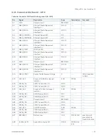
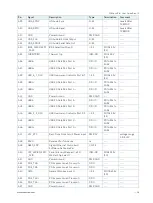
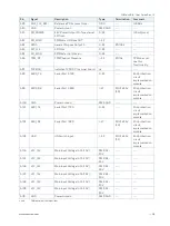
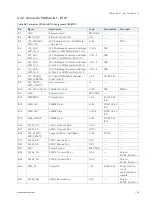
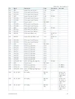
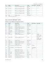
Pin
Signal
Description
Type
Termination
Comment
A58
P
PCI Express Lane 3 Tr
DP-O
---
---
A59
PCIE_TX3-
PCI Express Lane 3 Transmit -
DP-O
---
---
A60
GND
Power Ground
PWR GND
---
---
A61
P
PCI Express Lane 2 Tr
DP-O
---
---
A62
PCIE_TX2-
PCI Express Lane 2 Transmit -
DP-O
---
---
A63
GPI1
General Purpose Input 1
I-3.3
PU 100k 3.3V
(S0)
---
A64
P
PCI Express Lane 1 Tr
DP-O
---
---
A65
PCIE_TX1-
PCI Express Lane 1 Transmit -
DP-O
---
---
A66
GND
Power Ground
PWR GND
---
---
A67
GPI2
General Purpose Input 2
I-3.3
PU 100k 3.3V
(S0)
---
A68
P
PCI Express Lane 0 Tr
DP-O
---
---
A69
PCIE_TX0-
PCI Express Lane 0 Transmit -
DP-O
---
---
A70
GND
Power Ground
PWR GND
---
---
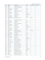
A71
LVDS Channel A DAT0+ / EDP Lane 2
Tr
DP-O
---
---
A72
LVDS_A0-
LVDS Channel A DAT0- / EDP Lane 2
Transmit -
DP-O
---
---
A73
LVDS Channel A DAT1+ / EDP Lane 1
Tr
DP-O
---
---
A74
LVDS_A1-
LVDS Channel A DAT1- / EDP Lane 1
Transmit -
DP-O
---
---
A75
LVDS Channel A DAT2+ / EDP Lane 0
Tr
DP-O
---
---
A76
LVDS_A2-
LVDS Channel A DAT2- / EDP Lane 0
Transmit -
DP-O
---
---
A77
LVDS_VDD_EN
LVDS / EDP Panel Power Control
O-3.3
PD 100k
---
A78
LVDS Channel A DAT3+
DP-O
---
---
A79
LVDS_A3-
LVDS Channel A DAT3-
DP-O
---
---
A80
GND
Power Ground
PWR GND
---
---
A81
LV
LVDS Channel A Clock+ / EDP Lane 3
Tr
DP-O
---
Clock: 20-80MHz
A82
LVDS_A_CK-
LVDS Channel A Clock- / EDP Lane 3
Transmit -
DP-O
---
Clock: 20-80MHz
A83
LVDS_I2C_CK
LVDS I2C Clock (DDC) / EDP AUX +
I/O-3.3
PU 2k2 3.3V
(S0)
---
A84
LVDS_I2C_DAT
LVDS I2C Data (DDC) / EDP AUX -
I/O-3.3
PU 2k2 3.3V
(S0)
---
A85
GPI3
General Purpose Input 3
I-3.3
PU 100k 3.3V
(S0)
---
A86
RSVD
Reserved for future use
nc
---
---
A87
eDP_HPD
EDP Hot Plug Detect
I-3.3
PD 400k
LVDS / 100k
EDP
---
A88
PCIE_
Reference PCI Express Clock +
DP-O
---
100MHz


