background image

COMe-cVR6 – User Guide Rev. 1.5 


www.kontron.com 


// 53 


8/


COMe Interface Connectors (X1A and X1B) 

The COMe-cVR6 is a COM Express® compact module containing two 220-pin connectors; each with two rows called 
row A & B on the primary connector and row C & D on the secondary connector.  


Figure 9: X1A and X1B COMe Interface Connectors 


8.1.


X1A and X1B Signals 

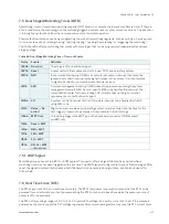
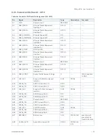
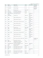
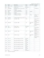
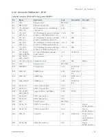
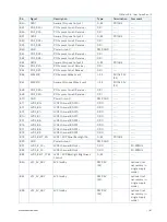
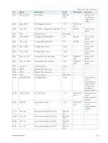
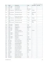
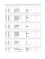
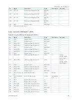
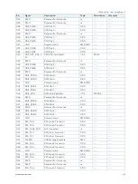
For a description of the terms used in the X1A and X1B pin assignment tables, see Table 63: General Signal Description 
or Appendix A, List of Acronyms. If a more detailed pin assignment description is required, refer to the PICMG 
specification COMe Rev 3.0 Type 6 standard. 


The information provided under type, module terminations and comments is complementary 
to the COM.0 Rev 3.0 Type 6 standard. For more information, contact Kontron Support. 


X1A 


Pin  

   D1 


Pin  

   A1 

X1B 

Summary of Contents for kontron COMe-cVR6

Page 1: ...USER GUIDE www kontron com 1 COMe cVR6 Doc User Guide Rev 1 5 Doc ID 1064 6276...

Page 2: ...COMe cVR6 User Guide Rev 1 5 www kontron com 2 This page has been intentionally left blank...

Page 3: ...be suitable for the specified use without further testing or modification Kontron expressly informs the user that this user guide only contains a general description of processes and instructions whic...

Page 4: ...quate design and operating safeguards You are solely responsible for compliance with all legal regulatory safety and security related requirements concerning your products You are responsible to ensur...

Page 5: ...formation refer to the corporate offices contact information on the last page of this user guide or visit our website CONTACT US Customer Support Find Kontron contacts by visiting http www kontron com...

Page 6: ...cribed by the law may endanger your life health and or result in damage to your material ESD Sensitive Device This symbol and title inform that the electronic boards and their components are sensitive...

Page 7: ...before performing any work on this product Earth ground connection to vehicle s chassis or a central grounding point shall remain connected The earth ground cable shall be the last cable to be discon...

Page 8: ...oduct then re pack it in the same manner as it was delivered Special care is necessary when handling or unpacking the product See Special Handling and Unpacking Instruction Quality and Environmental M...

Page 9: ...1 Commercial Grade Modules 0 C to 60 C 17 2 1 2 Extended Temperature Grade Modules E1 25 C to 75 C 17 2 1 3 Industrial Temperature Grade Modules E2 E2S 40 C to 85 C 18 2 2 Accessories 18 2 3 Functiona...

Page 10: ...vironmental Specification 45 5 1 1 Temperature 45 5 1 2 Humidity 45 5 2 Standards and Certifications 45 6 Mechanical Specification 47 6 1 1 Dimensions 47 6 1 2 Height 48 6 1 3 Heatspreader Dimension 4...

Page 11: ...ing 18 Table 4 Product Accessories COMe cVR6 18 Table 5 COMe Type 6 Accessories 18 Table 6 General Accessories 19 Table 7 Memory Modules 19 Table 8 Technical Data 21 Table 9 V1000 Processor Specificat...

Page 12: ...upported SPI Boot Flash Types for 8 SOIC Package 50 Table 62 Dual Stage Watchdog Timer Time out Events 51 Table 63 General Signal Description 54 Table 64 Connector X1A Row A Pin Assignment A1 A110 55...

Page 13: ...COMe cVR6 User Guide Rev 1 5 www kontron com 13 Figure 13 Security Setup Menu Initial Screen 80 Figure 14 Boot Screen 82 Figure 15 Save and Exit Setup Menu Initial Screen 83...

Page 14: ...Series processors Through the use of COM Express connectors the COMe cVR6 is easily exchangeable and offers the most flexibility for customers designing it into their embedded devices based on indivi...

Page 15: ...m x 95 mm c compact 95mm x 95 mm m mini 84 mm x 55 mm Processor code name VR AMD s Ryzen Embedded V and R Series Pinout type Type 6 Available temperature variants Commercial Extended E1 Industrial E2...

Page 16: ...FAN PWM out 1x 1x Express Card 2x 1 5 COM Express Benefits COM Express defines a Computer On Module or COM with all the components necessary for a bootable host computer packaged as a highly integrate...

Page 17: ...O DIMM Socket 36026 4000 20 4 COMe cVR6 V1605B 4G COM Express compact pin out type 6 Computer on Module with AMD V1605B 4x2 0 GHz 4GB memory down DDR4 SO DIMM Socket 36026 0000 20 4 COMe cVR6 V1605B C...

Page 18: ...umber Heatspreader validated ref types Description 36026 0000 99 0 HSP COMe cVR6 Cu core threaded Heatspreader for COMe cVR6 Cu core threaded mounting holes high performance 36026 0000 99 1 HSP COMe c...

Page 19: ...DA DP LVDS DP to LVDS adapter 96082 0000 00 0 KAB ADAPT DP DVI DP to DVI adapter cable 96083 0000 00 0 KAB ADAPT DP VGA DP to VGA adapter cable 96084 0000 00 0 KAB ADAPT DP HDMI DP to HDMI adapter cab...

Page 20: ...VR6 DDR4 2400 SODIMM 32GB ECC E2_CVR6 DDR4 2400 32GB ECC E2 260P 1200MHz PC4 2400 SODIMM 97031 1624 CVR6 DDR4 2400 SODIMM 16GB ECC E2_CVR6 DDR4 2400 16GB ECC E2 260P 1200MHz PC4 2400 SODIMM 97031 0824...

Page 21: ...C Staged Watchdog RTC BIOS AMI Aptio V Power Supply 8 5 V to 20 V Wide Range Single Supply Power Approtect Optional Wibu Code Meter ASIC connected to SoC USB Port 0 Wibu chip is only stuffed for optio...

Page 22: ...COMe cVR6 User Guide Rev 1 5 www kontron com 22 2 3 2 Block Diagram COMe cVR6 Figure 2 Block Diagram COMe cVR6...

Page 23: ...e CPU and up to a 107 improvement in Graphics performance Utilizing a 14 nm FinFET process the AMD Ryzen Embedded V1000 combines higher performance at comparable Thermal Design Power TDPs Up to four C...

Page 24: ...ssor Specifications Processor V1807B V1756B V1605B V1202B V1404B of Cores 4 4 4 2 4 of Threads 8 8 8 4 8 Processor Base Frequency 3 35 3 25 2 0 2 3 1 6 2 0 1T Boost Frequency 3 8 3 6 3 6 3 6 2 8 3 61...

Page 25: ...4K resolution via DisplayPort 1 4b and or HDMI 2 0b The integrated Video Hardware Accelerator supports decode or encode for various widely used video codecs with resolutions up to 4K AMD Ryzen Embedd...

Page 26: ...C 0 105 C PCI Lanes 8 Lanes Gen3 4x GPP 4x GFx 8 Lanes Gen3 4x GPP 4x GFx Max Channel dual Channel dual Channel 1 Nominal TDP 15 W configurable in BIOS 2 3 5 System Memory The system memory supports...

Page 27: ...R4 2400 Dual Rank DDR4 2400 V1404I Single Rank DDR4 2400 Dual Rank DDR4 2400 R1606G Single Rank DDR4 2400 Dual Rank DDR4 2400 R1505G Single Rank DDR4 2400 Dual Rank DDR4 2400 2 3 6 Graphics 2 3 6 1 Di...

Page 28: ...31 DP w Audio DP3 LVDS eDP option 1 DDI3 is not supported with R1505R R1606G SKUs Table 15 DDI1 Interfaces COMe Connector SoC Description DDI1_PAIR 0 3 DP0_TX 0 3 DDI1_PAIR 4 6 DDI1_CTRLCLK_AUX DP0_AU...

Page 29: ...lable as option which bypasses the eDP2LVDS bridge Table 19 eDP COMe Connector SoC Description LVDS_A_CK DP3_TX3 LVDS_A2 DP3_TX0 LVDS_A1 DP3_TX1 LVDS_A0 DP3_TX2 LVDS_I2C_CK DP3_AUXN LVDS_I2C_DAT DP3_A...

Page 30: ...used 2 3 9 I2C Bus Two I2C Buses are generated by FPGA s internal kCPLD block 1 External user accessible I2C connected to embedded EEPROM and COM Express connector a Optional SoC USBC I2C connected to...

Page 31: ...Reset CB_RESET COMe Signal SoC Pin Description CB_RESET SOC_PMU_RS T_1V8 Output to carrier Implemented in FPGA EC 2 3 14 System Reset SYS_RESET Table 27 System Reset SYS_RESET COMe Signal SoC Pin Des...

Page 32: ...0 SPI0_CS0 SPI0_CS1 Module 2 3 16 Speaker Out SPKR Table 30 Speaker Out SPKR COMe Signal SoC Pin Description SPKR SPKR AGPIO90 Speaker Buzzer out 2 3 17 Watchdog Timeout WDT Table 31 Watchdog Timeout...

Page 33: ...TPM LFRAME LPC_FRAME LRESET Generated in FPGA from PLTRST GPIO Not connected TPM_PP To COMe TPM_PP Pin 2 3 20 Onboard Fan Connector The analog output voltage on this connector is generated via a discr...

Page 34: ...There are also dependencies between GPP and GFX configuration 2 3 22 General Purpose PCI Express 3 0 R1000 SKUs The R1000 SKU processors support supports 4 or 8 GPP lanes up to Gen 3 depending of the...

Page 35: ...ed in different modes The Switch is used in a 6Port 6Lane Configuration 606 mode The routing is done in a different way regarding used SKU V1000 or R1000 Table 38 PCIe Switch V1000 COMe connector GPP...

Page 36: ...COMe cVR6 User Guide Rev 1 5 www kontron com 36 Figure 5 R1000 V1000 PCI Variants...

Page 37: ...ne Config PEG0 0 x4 x8 PEG1 1 PEG2 2 PEG3 3 PEG4 4 x4 PEG5 5 PEG6 6 PEG7 7 2 3 25 PCI Express Reference Clock Table 41 PCI Express Reference Clock COMe Connector SoC Pin PCIE_CK_REF GPP_CLK0 2 3 26 US...

Page 38: ...06G does support USB2 USB_SS2 by default DDI3 is not supported with R1000 SKUs R1505G R1606G does not support USB_SS3 USB3 just works as USB 2 0 Port 2 3 27 SATA The SATA high speed storage interface...

Page 39: ...d in Windows 10 can cause undefined LED behavior To disable ULP use the Intel ULPenable Utility 1 3 For more information refer to the EMD Customer Section or contact Kontron Support 2 3 31 BIOS Softwa...

Page 40: ...fic Product Features External I2C Bus Fast I2C 100 KHz 400 kHz MultiMaster capable Embedded API KEAPI3 Custom BIOS Settings Flash Backup Supported Watchdog Support Dual staged External SIO Supported o...

Page 41: ...1 Power Supply Rise Time The input voltage rise time is 0 1 ms to 20 ms from input voltage 10 to nominal VCC To comply with the ATX specification there must be a smooth and continuous ramp of each DC...

Page 42: ...still occurring Once the reset is asserted it remains asserted for 5 ms to 6 ms regardless of whether the SYS_RESET input remains asserted or not SM Bus Alert SMB_ALERT Pin B15 With an external batte...

Page 43: ...0 V To power on the module from S5 state press the power button or reconnect VCC Suspend Standby states are not supported in single supply mode Table 54 Single Supply Mode Settings State PWRBTN PWR_OK...

Page 44: ...ntal conditions Active or passive cooling solutions provided from Kontron for the COMe cVR6 are usually designed to cover the power and thermal dissipation for a commercial temperature range used in h...

Page 45: ...ertification Compliance Standard Definition Emission EMC EN 55022 Class B Information technology equipment Radio disturbance characteristics Limits and methods of measurement IEC EN 61000 6 3 Electrom...

Page 46: ...ent Including Electrical Business Equipment NWGQ2 E304278 NWGQ8 E304278 Shock IEC EN 60068 2 27 Non operating shock half sinusoidal 11 ms 15 g Vibration IEC EN 60068 2 6 Non operating vibration sinuso...

Page 47: ...cVR6 User Guide Rev 1 5 www kontron com 47 6 Mechanical Specification 6 1 1 Dimensions The dimensions of the module are 95 0 mm x 95 0 mm 3 75 x 3 75 Figure 6 Module Dimensions All dimensions shown i...

Page 48: ...a module height of approximately 13 mm from module PCB bottom to heatspreader top as shown in Figure 7 Module Height below Figure 7 Module Height 1 Heatspreader 2 Heatspreaader standoff s 3 Module PCB...

Page 49: ...xpress Computer On Modules imply BIOS support for the following external baseboard LPC Super I O controller features for the Winbond Nuvoton 3 3V 83627DHG P Table 59 Supported BIOS Features Winbond Nu...

Page 50: ...acturer Part Number Device ID 8 MB Macronix MX25L6406E 0x20 7 3 Fast I2C Fast I2C supports transfer between components on the same board The COMe cVR6 features an onboard I2C controller connected to t...

Page 51: ...specific BIOS code handles the interrupt The current BIOS handler for the watchdog SMI currently does nothing For special requirements contact Kontron Support 0100b SCI A system control interrupt SCI...

Page 52: ...he CPU Each TPM chip contains an RSA key pair called the Endorsement Key EK The pair is maintained inside the chip and cannot be accessed by software The Storage Root Key SRK is created when a user or...

Page 53: ...face Connectors 8 1 X1A and X1B Signals For a description of the terms used in the X1A and X1B pin assignment tables see Table 63 General Signal Description or Appendix A List of Acronyms If a more de...

Page 54: ...stor OA Output Analog PWR Power Connection OD Output Open Drain and Differential Pair To protect external power lines of peripheral devices make sure that the wires have the right diameter to withstan...

Page 55: ...A11 GND Power Ground PWR GND A12 GBE0_MDI0 Ethernet Media Dependent Interface 0 DP I O A13 GBE0_MDI0 Ethernet Media Dependent Interface 0 DP I O A14 GBE0_CTREF Center Tab Reference Voltage O 100nF cap...

Page 56: ...25k to 24 8k A41 GND Power Ground PWR GND A42 USB2 USB 2 0 Data Pair Port 2 DP I O PD 14 25k to 24 8k A43 USB2 USB 2 0 Data Pair Port 2 DP I O PD 14 25k to 24 8k A44 USB_2_3_OC USB Overcurrent Indicat...

Page 57: ...A0 LVDS Channel A DAT0 EDP Lane 2 Transmit DP O A73 LVDS_A1 LVDS Channel A DAT1 EDP Lane 1 Transmit DP O A74 LVDS_A1 LVDS Channel A DAT1 EDP Lane 1 Transmit DP O A75 LVDS_A2 LVDS Channel A DAT2 EDP La...

Page 58: ...it implemented on module A99 SER0_RX Serial Port 0 RXD I 5T PU 47k 3 3V S0 20V protection circuit implemented on module A100 GND Power Ground PWR GND A101 SER1_TX Serial Port 1 TXD O 3 3 20V protectio...

Page 59: ...B8 LPC_DRQ0 ESPI_ALERT0 LPC Serial DMA Master Request 0 eSPI Alert 0 I 3 3 PU 10k 3 3V B9 LPC_DRQ1 ESPI_ALERT1 Not connected nc B10 LPC_CLK ESPI_CK 24MHz LPC clock O 3 3 TBD 33MHz B11 GND Power Groun...

Page 60: ...current Indicator Port 4 5 I 3 3 PU 10k 3 3V S5 B39 USB5 USB 2 0 Data Pair Port 5 DP I O PD 14 25k to 24 8k B40 USB5 USB 2 0 Data Pair Port 5 DP I O PD 14 25k to 24 8k B41 GND Power Ground PWR GND B42...

Page 61: ...PU 10k 3 3V S5 B68 PCIE_RX0 PCI Express Lane 0 Receive DP I B69 PCIE_RX0 PCI Express Lane 0 Receive DP I B70 GND Power Ground PWR GND B71 LVDS_B0 LVDS Channel B DAT0 DP O B72 LVDS_B0 LVDS Channel B D...

Page 62: ...Data Channel Clock I O 5 PU 2k4 3 3 S0 Only on VGA Option B96 VGA_I2C_DATA Display Data Channel Data I O 5 PU 2k4 3 3 S0 Only on VGA Option B97 SPI_CS SPI Chip Select O 3 3 B98 RSVD Reserved for futur...

Page 63: ...C8 GND Power Ground PWR GND C9 USB_SSRX2 USB Super Speed Receive 2 DP I Only on DDI3x2_USBSS_ Port2 Option C10 USB_SSRX2 USB Super Speed Receive 2 DP I Only on DDI3x2_USBSS_ Port2 Option C11 GND Power...

Page 64: ...42 DDI3_PAIR1 DDI3 Pair 1 DP O C43 DDI3_PAIR1 DDI3 Pair 1 DP O C44 DDI3_HPD DDI3 Hotplug Detect I 3 3 PD 100k C45 RSVD Reserved for future use nc C46 DDI3_PAIR2 DDI3 Pair 2 DP O C47 DDI3_PAIR2 DDI3 Pa...

Page 65: ...cted nc C82 PEG_RX9 Not Connected nc C83 RSVD Reserved for future use nc C84 GND Power Ground PWR GND C85 PEG_RX10 Not Connected nc C86 PEG_RX10 Not Connected nc C87 GND Power Ground PWR GND C88 PEG_R...

Page 66: ...D Power Ground PWR GND D6 USB_SSTX1 USB Super Speed Transmit 1 DP O D7 USB_SSTX1 USB Super Speed Transmit 1 DP O D8 GND Power Ground PWR GND D9 USB_SSTX2 USB Super Speed Transmit 2 DP O Only on DDI3x2...

Page 67: ...P O D41 GND Power Ground PWR GND D42 DDI2_PAIR1 DDI2 Pair 1 DP O D43 DDI2_PAIR1 DDI2 Pair 1 DP O D44 DDI2_HPD DDI2 Hotplug Detect I 3 3 PD 100k D45 RSVD Reserved for future use nc D46 DDI2_PAIR2 DDI2...

Page 68: ...D81 PEG_TX9 Not Connected nc D82 PEG_TX9 Not Connected nc D83 RSVD Reserved for future use nc D84 GND Power Ground PWR GND D85 PEG_TX10 Not Connected nc D86 PEG_TX10 Not Connected nc D87 GND Power Gr...

Page 69: ...on Comment D106 VCC_12V Main Input Voltage 8 5 20V PWR 8 5 20V D107 VCC_12V Main Input Voltage 8 5 20V PWR 8 5 20V D108 VCC_12V Main Input Voltage 8 5 20V PWR 8 5 20V D109 VCC_12V Main Input Voltage 8...

Page 70: ...r splash screen 3 Press the DEL key 4 If the UEFI BIOS is password protected a request for password will appear Enter either the User Password or Supervisor Password see Chapter 9 2 4 Security Setup M...

Page 71: ...etup menu provides two main frames The left frame displays all available functions Configurable functions are displayed in blue Functions displayed in grey provide information about the status or the...

Page 72: ...Read only field Displays Module Information Product Name Revision Serial MAC Address Boot Counter and CPLD Rev Additional information for MAC Address The MAC address entry is the value used by the Eth...

Page 73: ...p menu Sub screens and Functions Sub Screen Function Second level Sub Screen Description Trusted Computing Security Device Support Enabled Disabled Pending Operation None TPM cleared Platform Hierarch...

Page 74: ...GPIOs in BIOS Enabled Disabled GPIO IRQ IRQ 3 15 Disabled I2C IRQ IRQ 3 15 Disabled IDE Configuration SATA Port0 5 Not Present PCIe Port Configuration PCIe Port Control Enabled Disabled Device 1 Fun...

Page 75: ...lect DFP1_DP Debug Port Table Configuration Debug Port Table Enabled Disabled Debug Port Table 2 Enabled Disabled SIO Configuration Active Serial Port 1 or 2 Use This Device Enabled Disabled Possible...

Page 76: ...54 W Audio IOs Auto Max HDA Max mHDA Max Soundwire MinHDA Max Soundwire Min mHDA I2S Disable Audio IOs Soundwire FCH Common Options SATA Configuration Options SATA Controller Auto Disabled Enabled SA...

Page 77: ...ion PCIe GPP Port Config 1x2 4x1 2x1 1x4 2x1 2x1 1x2 Disk Devices Group RAM Disk Configuration Disk Memory Type Boot Service Data Reserved Create raw Size 1 Create Discard Exit Create from file Remove...

Page 78: ...n Function Second level Sub Screen Description South Bridge SB USB Configuration XHCI0 Port 0 1 2 3 Enabled Disabled XHCI1 Port 0 1 Enabled Disabled SB Power Saving AB Clock Gating Auto Enabled Disabl...

Page 79: ...esolution Auto VGA WGA XGA WXGA WSVGA SXGA UXGA WUXGA FHD Custom Panel Channel Mode Auto Single Dual Backlight Control PWM None PWM Inverted I2C Inverted PWM Frequency 200 Hz 400 Hz 1 kHz 40 kHz Backl...

Page 80: ...are case sensitive Figure 13 Security Setup Menu Initial Screen Table 72 Security Setup Menu Functions Function Description Administrator Password Sets administrator password User Password Sets user p...

Page 81: ...he user s password is set then the password is a power on password and must be entered to boot or enter setup In the setup the user has administrator rights The required password length in characters...

Page 82: ...pt Timeout 1 Bootup NumLock State On Off Quiet Boot Enabled Disabled Boot Option Priorities Boot Option 1 UEFI Built in EFI Shell Disabled Fast Boot Enabled Disabled SATA Support Last Boot HDD Only Al...

Page 83: ...Changes and Exit Exits system setup without saving changes Save Changes and Reset Resets system after saving changes Discard Changes and Reset Resets system setup without saving changes Save Changes S...

Page 84: ...Shell forms an entry into the UEFI boot order and is the first boot option by default 9 3 1 1 Entering the UEFI Shell To enter the UEFI Shell follow the steps below 1 Power on the board 1 Press the F7...

Page 85: ...up script terminates then the default boot order is continued 9 4 2 Create a Startup Script Startup scripts can be created using the UEFI Shell built in editor edit or under any OS with a plain text e...

Page 86: ...Addition connected hardware full description of hardware set up Be ready to explain the nature of your problem to the service technician The serial number can be found on the Type Label located on the...

Page 87: ...or Kontron Europe GmbH and fill out the form Take care to include a short detailed description of the observed problem or failure and to include the product identification Information Name of product...

Page 88: ...ble Unit Gb Gigabit GBE Gigabit Ethernet GPI General Purpose Input GPIO General Purpose Input Output GPO General Purpose Output GPU Graphics Processing Unit HBR2 High Bitrate 2 HDA High Definition Aud...

Page 89: ...all Outline Dual in line Memory Module SOIC Small Outline Integrated Circuit SOL Serial Over LAN SPI Serial Peripheral Interface SSH Secure Shell TPM Trusted Platform Module UART Universal Asynchronou...

Page 90: ...ts and tailor made solutions based on highly reliable state of the art embedded technologies Kontron provides secure and innovative applications for a variety of industries As a result customers benef...

Reviews: