1-3 Precautions for Electrostatically Sensitive Devices (ESDs)
1. Some semiconductor (“solid state”) devices
are easily damaged by static electricity. Such
components are called Electrostatically
Sensitive Devices (ESDs); examples include
integrated circuits and some field-effect
transistors. The following techniques will
reduce the occurrence of component damage
caused by static electricity.
2. Immediately before handling any semicon
ductor components or assemblies, drain the
electrostatic charge from your body by
touching a known earth ground. Alternatively,
wear a discharging wrist-strap device. (Be
sure to remove it prior to applying power—
this is an electric shock precaution.)
3. After removing an ESD-equipped assembly,
place it on a conductive surface such as
aluminum foil to prevent accumulation of
electrostatic charge.
4. Do not use freon-propelled chemicals. These
can generate electrical charges that damage
ESDs.
5. Use only a grounded-tip soldering iron when
soldering or unsoldering ESDs.
6. Use only an anti-static solder removal device.
Many solder removal devices are not rated as
“anti-static”; these can accumulate sufficient
electrical charge to damage ESDs.
7. Do not remove a replacement ESD from its
protective package until you are ready to
install it. Most replacement ESDs are
packaged with leads that are electrically
shorted together by conductive foam,
aluminum foil or other conductive materials.
8. Immediately before removing the protective
material from the leads of a replacement ESD,
touch the protective material to the chassis or
circuit assembly into which the device will be
installed.
9. Minimize body motions when handling
unpackaged replacement ESDs. Motions such
as brushing clothes together, or lifting a foot
from a carpeted floor can generate enough
static electricity to damage an ESD.
Precautions
1-4
Samsung Electronics
CAUTION
These servicing instructions are for use by
qualified service personnel only.
To reduce the risk of electric shock do not
perform any servicing other than that contained
in the operating instructions unless you are
qualified to do so.
Summary of Contents for ST55W3PCX/XAX
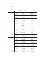
Page 10: ...Reference Information 2 4 Samsung Electronics 2 3 IC Line Up 2 3 1 Progressive ...
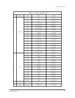
Page 11: ...Reference Information Samsung Electronics 2 5 ...
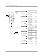
Page 12: ...Reference Information 2 6 Samsung Electronics 2 4 MICOM IIC BUS LINE UP ...
Page 14: ...MEMO 3 2 Samsung Electronics ...
Page 52: ...MEMO 4 38 Samsung Electronics ...
Page 56: ...MEMO 5 4 Samsung Electronics ...
Page 87: ...Schematic Diagrams 10 2 Samsung Electronics TP20 TP03 TP04 10 2 MAIN 2 TP03 TP04 TP20 ...
Page 88: ...Samsung Electronics Schematic Diagrams 10 3 10 3 MAIN 3 TP12 TP13 TP12 TP13 ...
Page 90: ...Samsung Electronics Schematic Diagrams 10 5 10 5 MICOM ...
Page 91: ...Schematic Diagrams 10 6 Samsung Electronics 10 6 CRT ...
Page 92: ...Samsung Electronics Schematic Diagrams 10 7 10 7 SUB 1 TP21 TP21 ...
Page 93: ...Schematic Diagrams 10 8 Samsung Electronics 10 8 SUB 2 TP24 TP23 TP22 TP22 TP23 TP24 ...
Page 94: ...Samsung Electronics Schematic Diagrams 10 9 10 9 CONVERGENCE SDC12 1 ...
Page 95: ...Schematic Diagrams 10 10 Samsung Electronics 10 10 CONVERGENCE SDC12 2 ...
Page 96: ...Samsung Electronics Schematic Diagrams 10 11 10 11 PRO SCAN 1 ...
Page 97: ...Schematic Diagrams 10 12 Samsung Electronics 10 12 PRO SCAN 2 ...
Page 98: ...Samsung Electronics Schematic Diagrams 10 13 10 13 PRO SCAN 3 ...
Page 99: ...Schematic Diagrams 10 14 Samsung Electronics 10 14 PRO SCAN 4 ...
Page 100: ...10 15 CG AMP Samsung Electronics Schematic Diagrams 10 15 ...
Page 101: ...Schematic Diagrams 10 16 Samsung Electronics 10 16 AV FRONT ...
Page 102: ...10 17 CONTROL Samsung Electronics Schematic Diagrams 10 17 ...
Page 103: ...Schematic Diagrams 10 18 Samsung Electronics 10 18 DY JACK SENSOR DY JACK SENSOR ...


