


CONTROL REGISTERS
S3C80M4/F80M4
4-8
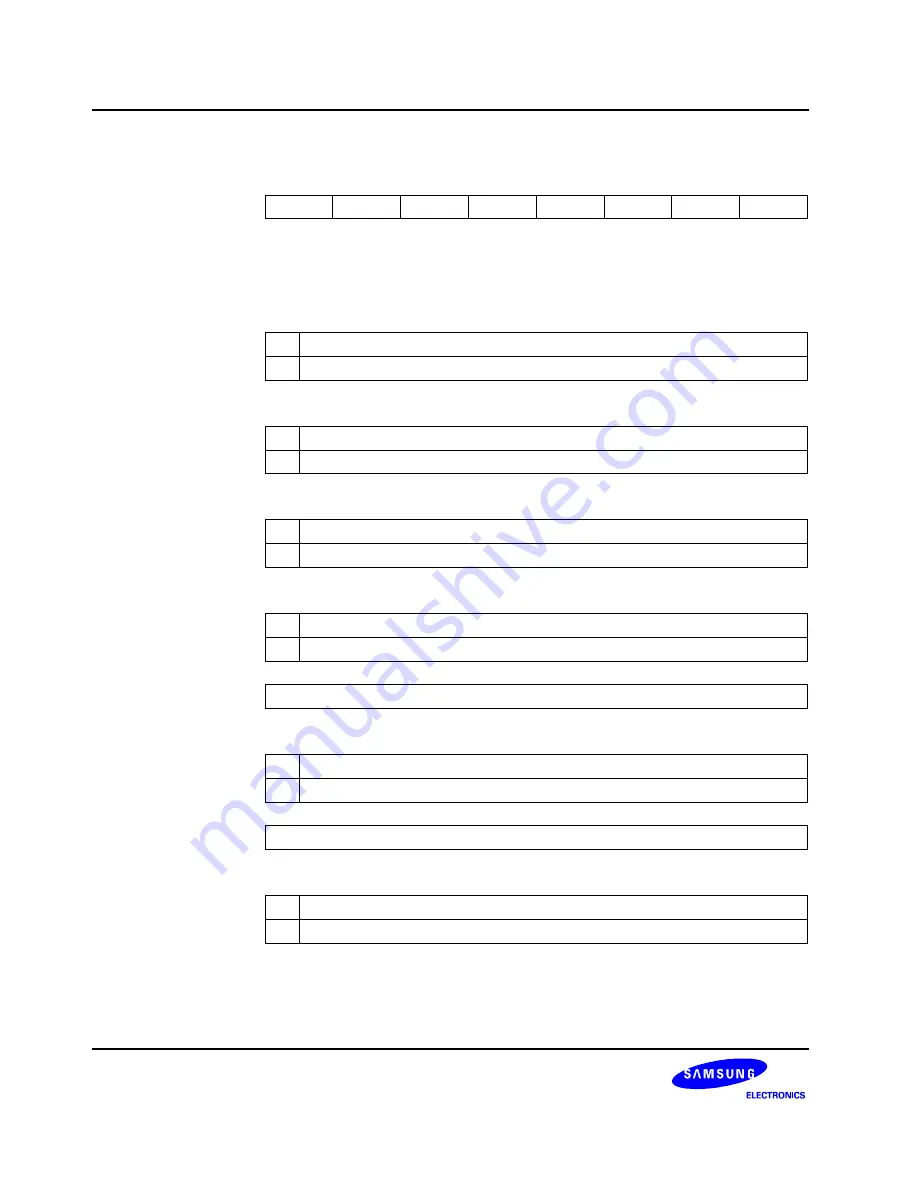
IMR
— Interrupt Mask Register
DDH
Set 1
Bit
Identifier
.7 .6 .5 .4 .3 .2 .1 .0
RESET Value
x x x x x x x x
Read/Write
R/W R/W R/W R/W R/W R/W R/W R/W
Addressing Mode
Register addressing mode only
.7
Interrupt Level 7 (IRQ7) Enable Bit; External Interrupts P0.3
0 Disable
(mask)
1 Enable
(unmask)
.6
Interrupt Level 6 (IRQ6) Enable Bit; External Interrupts P0.2
0 Disable
(mask)
1 Enable
(unmask)
.5
Interrupt Level 5 (IRQ5) Enable Bit; External Interrupts P0.1
0 Disable
(mask)
1 Enable
(unmask)
.4
Interrupt Level 4 (IRQ4) Enable Bit; External Interrupts P0.0
0 Disable
(mask)
1 Enable
(unmask)
.3
Reserved
.2
Interrupt Level 2 (IRQ2) Enable Bit; PWM
0 Disable
(mask)
1 Enable
(unmask)
.1
Reserved
.0
Interrupt Level 0 (IRQ0) Enable Bit; Timer 0 Match
0 Disable
(mask)
1 Enable
(unmask)
NOTE:
When an interrupt level is masked, any interrupt requests that may be issued are not recognized by the CPU.
Summary of Contents for S3C80M4/F80M4
Page 1: ...S3C80M4 F80M4 8 BIT CMOS MICROCONTROLLERS USER S MANUAL Revision 1 ...
Page 44: ...ADDRESS SPACES S3C80M4 F80M4 2 20 NOTES ...
Page 84: ...CONTROL REGISTERS S3C80M4 F80M4 4 26 NOTES ...
Page 102: ...INTERRUPT STRUCTURE S3C80M4 F80M4 5 18 NOTES ...
Page 190: ...INSTRUCTION SET S3C80M4 F80M4 6 88 NOTES ...
Page 202: ...RESET and POWER DOWN S3C80M4 F80M4 8 6 NOTES ...
Page 216: ...8 BIT TIMER 0 S3C80M4 F80M4 11 4 NOTES ...
Page 220: ...8 BIT PULSE WIDTH MODULATION S3C80M4 F80M4 12 4 NOTES ...
Page 230: ...ELECTRICAL DATA S3C80M4 F80M4 13 10 NOTES ...


