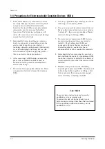
1-4 Precautions for Electrostatically Sensitive Devices (ESDs)
1. Some semiconductor (“solid state”) devices
are easily damaged by static electricity. Such
components are called Electrostatically
Sensitive Devices (ESDs); examples include
integrated circuits and some field-effect
transistors. The following techniques will
reduce the occurrence of component damage
caused by static electricity.
2. Immediately before handling any semicon
ductor components or assemblies, drain the
electrostatic charge from your body by
touching a known earth ground. Alternatively,
wear a discharging wrist-strap device. (Be
sure to remove it prior to applying power—
this is an electric shock precaution.)
3. After removing an ESD-equipped assembly,
place it on a conductive surface such as
aluminum foil to prevent accumulation of
electrostatic charge.
4. Do not use freon-propelled chemicals. These
can generate electrical charges that damage
ESDs.
5. Use only a grounded-tip soldering iron when
soldering or unsoldering ESDs.
6. Use only an anti-static solder removal device.
Many solder removal devices are not rated as
“anti-static”; these can accumulate sufficient
electrical charge to damage ESDs.
7. Do not remove a replacement ESD from its
protective package until you are ready to
install it. Most replacement ESDs are
packaged with leads that are electrically
shorted together by conductive foam,
aluminum foil or other conductive materials.
8. Immediately before removing the protective
material from the leads of a replacement ESD,
touch the protective material to the chassis or
circuit assembly into which the device will be
installed.
9. Minimize body motions when handling
unpackaged replacement ESDs. Motions such
as brushing clothes together, or lifting a foot
from a carpeted floor can generate enough
static electricity to damage an ESD.
Precautions
1-4
Samsung Electronics
CAUTION
These servicing instructions are for use by
qualified service personnel only.
To reduce the risk of electric shock do not
perform any servicing other than that contained
in the operating instructions unless you are
qualified to do so.
Summary of Contents for PPM42S2X/XAA
Page 2: ...ELECTRONICS Samsung Electronics Co Ltd APR 2002 Printed in Korea AA82 ...
Page 10: ...3 2 Samsung Electronics MENO ...
Page 25: ...Circuit Operation Description Samsung Electronics 5 3 5 1 2 D PDP PS 42 BLOCK DIAGRAM ...
Page 38: ...Circuit Operation Description 5 16 Samsung Electronics 5 2 3 D DRIVER CIRCUIT DIAGRAM ...
Page 39: ...Circuit Operation Description Samsung Electronics 5 17 5 2 3 E DRIVER BOARD CONNECTOR LAYOUT ...
Page 40: ...Circuit Operation Description 5 18 Samsung Electronics ...
Page 41: ...Circuit Operation Description Samsung Electronics 5 19 ...
Page 42: ...Circuit Operation Description 5 20 Samsung Electronics ...
Page 43: ...Circuit Operation Description Samsung Electronics 5 21 ...
Page 44: ...Circuit Operation Description 5 22 Samsung Electronics ...
Page 45: ...Circuit Operation Description Samsung Electronics 5 23 ...
Page 46: ...Circuit Operation Description 5 24 Samsung Electronics ...
Page 47: ...Circuit Operation Description Samsung Electronics 5 25 ...
Page 48: ...Circuit Operation Description 5 26 Samsung Electronics ...
Page 49: ...Circuit Operation Description Samsung Electronics 5 27 ...
Page 50: ...Circuit Operation Description 5 28 Samsung Electronics ...
Page 51: ...Circuit Operation Description Samsung Electronics 5 29 ...
Page 52: ...Circuit Operation Description 5 30 Samsung Electronics ...
Page 82: ...Circuit Operation Description 5 60 Samsung Electronics ...
Page 83: ...Circuit Operation Description Samsung Electronics 5 61 ...
Page 84: ...Circuit Operation Description 5 62 Samsung Electronics MEMO ...
Page 93: ...Exploded View Parts List Samsung Electronics 7 1 7 Exploded View Parts List 7 1 PPM42S2X XAA ...
Page 106: ...Electrical Parts List 8 12 Samsung Electronics MEMO ...
Page 128: ...10 14 Samsung Electronics MEMO ...
Page 130: ...11 2 Samsung Electronics MENO ...
Page 133: ...Samsung Electronics Schematic Diagrams 12 3 TP01 12 3 SCALER3 3D COMB FILTER TP01 CVBS IN ...
Page 134: ...Schematic Diagrams 12 4 Samsung Electronics 12 4 SCALER4 VIDEO DECODER PIP FIRST IN OUTPUT ...
Page 135: ...Samsung Electronics Schematic Diagrams 12 5 12 5 SCALER5 VIDEO DA CON ...
Page 141: ...Samsung Electronics Schematic Diagrams 12 11 12 11 SOUND ...
Page 143: ...Samsung Electronics Schematic Diagrams 12 13 12 13 CONTROL REMOCON CONTROL REMOCON ...


