background image

10-10

Samsung Electronics

Glossary

Reset 

:

(Refer to erase.)

Reset discharge, Reset pulse 

:

(Refer to erase.) 

Resolution 

:

Display’s ability to enable to distinguish the matters close to each other. It is confusing with addressibility
that generates pattern undistinguishable to the eyes.

Row electrodes 

:

Horizontally successive electrodes. In terms of traditional drive concept, these are the sustained electrodes.
If the panel is installed toward portrait, these row electrodes can be arranged horizontally.   

Sand discharge 

:

Process where grinding of surface occurs. It is used for making three dimensional surface in lithography or
silt in sheet. 

Scan discharge 

:

Discharge injected along the pair of sustained electrodes.

Scan electrode 

:

Electrodes of the pair of sustained electrodes that inject discharge downward along the panel columns.

Scan pulse 

:

Waveform that injects discharge with new columns. 
Optic defects where scratches display over certain size. 

Seal 

:

Combining the substrates or substrate with ventilation tube.

Seal layer 

:

Material layer that provides the connection of substrates. This can be a single layer of solder glass (frit) or
the combination of solder glass and ring.

Sealing 

:

Process where free electrons that get out of the surface by extracting static electricity field when energetic
electrons or ions are limited to a surface. 

Secondary electron emission 

:

Process where drags discharged cell to certain waveform. This could occur before ionization offset when
cell voltage decreases.

Self erase 

:

Plasma display in the form where stimulating discharge occurs for discharge process precedes below panel.  

Self-scan type PDP 

:

Plasma display in the form where stimulating discharge occurs for discharge process precedes below panel.

Self-shift type PDP 

:

Process of combining substrates. High temperature process that melts solder glass combining substrates.

Summary of Contents for PPM42S2X/XAA

Page 1: ...CONTENTS Precautions Reference Information Specifications Alignment and Adjustments Circuit Operation Description Troubleshooting Exploded View and Parts List Electric Parts List Handling Description Glossary Wiring Diagram Schematic Diagrams 1 2 3 4 5 6 7 8 9 10 11 12 ...

Page 2: ...ELECTRONICS Samsung Electronics Co Ltd APR 2002 Printed in Korea AA82 ...

Page 3: ...rectly into the power outlet With the unit s AC switch first in the ON position and then OFF measure the current between a known earth ground metal water pipe conduit etc and all exposed metal parts including antennas handle brackets metal cabinets screwheads and control shafts The current measured should not exceed 3 5 milliamp Reverse the power plug prongs in the AC outlet and repeat the test Fi...

Page 4: ...ondary ground system in addition to the main chassis ground This secondary ground system is not isolated from the AC power line The two ground systems are electrically separated by insulating material that must not be defeated or altered 13 Components parts and wiring that appear to have overheated or that are otherwise damaged should be replaced with parts that meet the original specifications Al...

Page 5: ...o the unit or any of its assemblies unless all solid state heat sinks are correctly installed 7 Always connect a test instrument s ground lead to the instrument chassis ground before connecting the positive lead always remove the instrument s ground lead last 8 Plasma display panels have partial afterim ages when a same picture continues to be dis played for a certain time This happens due to the ...

Page 6: ...oldering iron when soldering or unsoldering ESDs 6 Use only an anti static solder removal device Many solder removal devices are not rated as anti static these can accumulate sufficient electrical charge to damage ESDs 7 Do not remove a replacement ESD from its protective package until you are ready to install it Most replacement ESDs are packaged with leads that are electrically shorted together ...

Page 7: ...rtz Hour Inches Per Second Kilowatt hour Kilogram Kilohertz Kilohm Kilometer Kilometer Per Hour Kilovolt Kilovolt ampere Kilowatt Liter Megahertz MV MW MΩ m µA µF µH µm µs µW mA mg mH mI mm ms mV nF Ω pF Ib rpm rps s V VA W Wh Megavolt Megawatt Megohm Meter Microampere Microfarad Microhenry Micrometer Microsecond Microwatt Milliampere Milligram Millihenry Milliliter Millimeter Millisecond Millivol...

Page 8: ...afe Ground Green Y High High Frequency High Fidelity Inductance Capacitance Integrated Circuit Intermediate Frequency I O L L LED LF MOSFET MTS NAB NEC NTSC OSD PCB PLL PWM QIF R RC RF R Y SAP SAW SIF SMPS S N SW TP TTL TV UHF UL UV VCD VCO VCXO VHF VIF VR VTR VTVM TR Input output Left Low Light Emitting Diode Low Frequency Metal Oxide Semiconductor Field Effect Tr Multi channel Television Sound N...

Page 9: ...put AUDIO Output VIDEO Input Dimensions mm inch Weight PPM42S2 1038 8 W x 89 D x 635 H mm 40 9 W x 3 5 D x 25 H Inches 54 W x 31 5 D x 220 H mm 2 13 W x 1 24 D x 8 66 H Inches 32Kg 70 55 bs 150g Including batteries 0 33 bs AC 100 240V 50 60Hz 310 Watts 852 H X 480 V 106Cm 42 Inches VIDEO S VIDEO COMPONENT PC RGB 7W 7W 8Ω VIDEO S VIDEO COMPONENT 1 480i 2 480p 720p 1080i PC RGB 1 D SUB RGB 2 BNC ...

Page 10: ...3 2 Samsung Electronics MENO ...

Page 11: ...sful repeat the procedures above 4 1 2 Initial DISPLAY State in times of SERVICE MODE Switch overs 4 1 2 A OSD DISPLAY 4 1 2 B BUTTONS OPERATIONS WITHIN SERVICE MODE 1 PWS364 9 Pinp Control 2 VPC3230 10 OSD Position 3 SDA9400 11 Test Pattern 4 SDA9280 12 Option Table 5 AD9884 Video 13 Reset 6 AD9884 DTV PC 7 CXA2101Q 1 8 CXA2101Q 2 Release Time Menu Joystick UP DOWN Joystick LEFT RIGHT Entire menu...

Page 12: ...tion Red Gain Green Gain Blue Gain Red Offset Green Offset Blue Offset APL On Off High Light Low Light Shit Pixel Test Pixel Number Shift Line Time 93 35 113 113 113 139 139 139 1 113 139 on 0 4 4 4 Default of MODE VIDEO S VHS Component1 Component2 PC 30 34 148 148 148 133 133 133 1 148 133 on 0 4 4 4 27 20 125 125 125 129 129 129 1 125 129 on 0 4 4 4 ...

Page 13: ...ight 3230 Contrast H LPF Y C LPF2 H LPF Chroma CBW2 H Peaking Filter Coaring Off On PK Default of MODE 195 27 2 3 1 1 4 146 45 0 0 1 1 3 195 27 2 3 1 1 4 146 45 0 0 2 1 3 VIDEO S VHS Component1 Component2 PC DO NOT ENTER No OSD 4 1 3 C SDA9400 1 2 3 4 5 6 SNR On VCSNR On HCSNR On DTNR On TNRCLY TNRCNC Default of MODE 1 1 0 1 5 5 VIDEO S VHS Component1 Component2 PC DO NOT ENTER No OSD ...

Page 14: ...ult of MODE 0 0 11 7 11 12 2 1 VIDEO S VHS Component1 Component2 PC DO NOT ENTER 4 1 3 E AD9884 1 2 3 4 5 6 7 Red Gain Green Gain Fix Blue Gain Red Offset Green Offset Fix Blue Offset Current Default of MODE 142 132 143 28 32 21 143 132 143 38 32 25 1 VIDEO S VHS Component1 Component2 PC 4 1 3 D SDA9280 No OSD No OSD 145 132 137 34 32 27 ...

Page 15: ... PC No OSD 1 2 3 4 5 6 7 8 9 10 11 12 13 14 15 16 17 18 Sub Bright Limit Level System D Color R Drive G Drive B Drive R Cutoff G Cutoff B Cutoff ABL Mode ABL TH H sep sel Fix Sync V Time Con H Width HHD Time Con Picture 52 0 2 1 32 32 32 32 32 32 0 0 0 0 1 1 0 10 52 0 1 1 32 32 32 32 32 32 0 0 0 0 1 1 0 10 DO NOT ENTER ...

Page 16: ...t1 Component2 PC No OSD 1 2 3 4 5 6 7 8 9 10 11 12 13 14 15 16 17 18 HS Mask Sub Cont Sub Color Sub Hue Sub SHP R Y R R Y B G Y R G Y B PABL Level SHP FO Pre Over CTI Level LTI Level DC Tran D Pic Color Brightness 1 7 14 6 2 7 14 6 7 6 2 0 1 0 1 2 26 35 1 8 14 5 2 7 14 12 5 6 2 0 1 0 2 3 26 37 DO NOT ENTER ...

Page 17: ...sung Electronics 4 7 4 1 3 H PinP Control 1 2 3 4 5 6 7 Pip HPos Pip VPos Bright YUV Cont YUV Luma Delay 3230 Bright 3230 Contrast Default of MODE 6 13 195 27 0 40 38 6 13 195 27 0 40 38 VIDEO S VHS Component1 Component2 PC No OSD ...

Page 18: ...LOW light as Low Light 7 Adjust HIGH light as High Light W B Adjustment SPEC Suwon Factory Toshiba PATTERN Condition of Signals Video S VHS Component1 DVD 10 Gray 0 1 3 4 5 7 8 9 10 ShibaSoku TG71BX Component 2 DTV 9 Gray 0 1 3 4 5 7 8 9 LT446 1080i output PC 16 Gray 0 1 2 4 5 6 7 8 10 15 TP36B W B x y Y fL T K VIDEO 10 Gray D T V 9 Gray P C 16 Gray High Low High Low High Low Picture Quality Asses...

Page 19: ...P N N P P Video Signal Dot Line 70 086 85 080 85 080 70 087 85 039 59 940 72 809 75 000 85 008 60 000 60 000 56 250 60 317 72 188 75 000 85 061 60 004 70 069 75 029 84 997 31 469 37 861 37 861 31 469 37 927 31 469 37 861 37 500 43 269 29 800 31 731 35 156 37 879 48 077 46 875 53 674 48 363 56 476 60 023 68 677 N N P P P N N N N N P N N P P P P P N N P P Vertical Frequency Hz Horizontal Frequency K...

Page 20: ...ving related Board Layou Voltage Adjustments n Adjust all of variable resistances except V9 VG clockwise to decrease the voltage n n For PPM42S2 models readjust VR 6V to 5 9V 0 2V n When replacing the X Y driving boards avoid waveform adjustments using variable resistance as they have been adjusted according to the characteristics of PDP panel ...

Page 21: ...evered 1 DIODE 2 TRANSISTOR l For NPN KSC815 Y 2SC2068 2SC2331 Y l For PNP KSA539 Y Forward Direction Hundreds of ohms Reverse Direction Infinity Between Anode and Cathode C COLLECTOR E B BASE B C C COLLECTOR E B BASE B C E EMITTER E EMITTER Forward Direction Hundreds of ohms Hundreds of ohms Infinity Reverse Direction Infinity Infinity Infinity Between B and E Between B and C Between E and C Forw...

Page 22: ...st overvoltage in PIN Generally except for internal circuit defects IC defects can be found by measuring the DIODE Defects have SHORT 0 ohm for both forward and reverse direction Hundreds of ohms Forward Direction Reverse Direction Varying depending on IC but generally normal Infinity in DIODE TEST MODE ...

Page 23: ...IFICATION 5 1 2 A INPUT PDP 42PS board is designed so that input power can be used within AC 90 VAC to 264 VAC with 50 60Hz 3Hz 5 1 2 B OUTPUT PDP 42PS board provides 13 output switching power supplies 165Vs 220Set 185Ve 75Va 80Scan 18Vg 5Vsb 5V D 5 9V A 12V 9V 12Vfan and 12Vsamp The output voltage and current requirements for continuous operation are stated below Table 3 Table1 Specifications of ...

Page 24: ...n 90 VAC to 264VAC 3 Embedded thermal sensor The board is equipped with thermal sensor to detect the internal temperature of the unit and to short relay when the internal temperature is higher than specified temperature so as to shutdown the unit 4 Improvement of power factor The board is designed using PFC circuit so that PF Power Factor can be over 0 95 because low PF can be a problem in high vo...

Page 25: ...Circuit Operation Description Samsung Electronics 5 3 5 1 2 D PDP PS 42 BLOCK DIAGRAM ...

Page 26: ...Vscan V12 and Vg Vset Ve and Vscan used DC DC module V D Va V12 and Vfan used forward converter and Vsamp used flyback converter V A V9 and Vg are simply implemented using switching regulator 5 1 3 Requirements of PDP SMPS Since SMPS does not operate alone but it operates with the load of the whole system it should be designed carefully considering the load of the system In addition it should be d...

Page 27: ...Pi is determined by the addition of output power consumption Po and internal power loss of SMPS Pl Provided that the power conversion efficiency is _ If the power conversion efficiency of 100W SMPS is 70 the internal power loss is about 42 8W by Equation 1 If the power conversion efficiency of 400W SMPS for 42 SD is 82 the internal power loss is 87 8W by Equation 1 Table 4 shows internal power los...

Page 28: ...nce of voltage occurs and finally a power capacitor or a transformer generates heat fire or noise occurs controls malfunction or the accessed devices abnor mally operate or their lives are shortened To prevent those symptoms IEC International Electrotechnical Commission regulated standards for Power Supply Harmonics Refer to IEC 1000 3 2 Figure 8 shows the basic structure of Active Boost PFC and w...

Page 29: ...weight high power consumption power design it is hard to be used when stability and precise control are required Power stage for PDP can be designed using the lightweight SMPS feature It is important to design SMPS considering system load stability and related international standards The architecture and the pulse of active boost PFC ...

Page 30: ...ess and sustaining sections is most widely used to generate the drive pulse Discharges conducted within PDP pixels using this method can largely be classi fied into 3 types as follows 1 Address discharge This functions to generate wall voltage within pixels to be lighted by addressing information to them i e impressing data voltage 2 Sustain discharge This means a display section where only pixels...

Page 31: ...gative wall charge The address discharge serves to generate wall voltage in pixels where images are to be displayed that is discharge is to be generated prior to the sustaining discharge section Namely pixels with wall voltage by the address discharge will generate sustaining discharge by the following sustaining pulses 3 Erase discharge The purpose of resetting or erase discharge is to make even ...

Page 32: ...Circuit Operation Description 5 10 Samsung Electronics 5 2 2 SPECIFICATION OF DRIVE PULSES 5 2 2 A DRIVE PULSES ...

Page 33: ...al to the upcoming address discharge 4 Y scan pulse This is called the scan pulse selecting each of Y electrodes on a one line at a time basis In this case Vscan means the scan bias voltage About 70 V Vscan voltage is impressed on the selected electrode lines while 0 V GND voltage is impressed on the other lines In the cells the address pulse 70V 75V is impressed on address discharge is occurred b...

Page 34: ... 4 scan driver IC s STMicroelectronics STV7617 with 64 or 65 outputs 4 COF Impresses Va pulse on address electrodes in the address section and generates address discharge based on a difference between such Va pulse and scan pulse impressed on Y electrodes It is in the form of COF and a COF is equipped with 4 data drive IC s STMicroelectronics STV7610A with 96 outputs For a single scan 7 COF s are ...

Page 35: ...Circuit Operation Description Samsung Electronics 5 13 5 2 3 B DRIVING BOARD S BLOCK DIAGRAM POWER 17V 75V 220V 170V POWER 220V 170V 17V 1 Y 2 X ...

Page 36: ...operations 1 Power supply 1 Supplied from the power supply board For sustaining discharge 180V For logic signaling buffer 5V and For gate driver IC 15V 2 Generated by the internal DC DC part For generating Vw pulse 180V 2 Logic signal 1 Supplied from the logic board Gate signals for FETs ...

Page 37: ...2 FET2 gets short circuited thereby causing GND to be outputted to output terminals 2 With signal impressed on G1 FET1 gets short circuited and with no signal impressed on G2 FET2 gets open circuited thereby causing 180V to be outputted to output terminals 1 With signal impressed on the gate Positive voltage FET gets short circuited a conducting wire of zero 0 resistance and 2 With no signal impre...

Page 38: ...Circuit Operation Description 5 16 Samsung Electronics 5 2 3 D DRIVER CIRCUIT DIAGRAM ...

Page 39: ...Circuit Operation Description Samsung Electronics 5 17 5 2 3 E DRIVER BOARD CONNECTOR LAYOUT ...

Page 40: ...Circuit Operation Description 5 18 Samsung Electronics ...

Page 41: ...Circuit Operation Description Samsung Electronics 5 19 ...

Page 42: ...Circuit Operation Description 5 20 Samsung Electronics ...

Page 43: ...Circuit Operation Description Samsung Electronics 5 21 ...

Page 44: ...Circuit Operation Description 5 22 Samsung Electronics ...

Page 45: ...Circuit Operation Description Samsung Electronics 5 23 ...

Page 46: ...Circuit Operation Description 5 24 Samsung Electronics ...

Page 47: ...Circuit Operation Description Samsung Electronics 5 25 ...

Page 48: ...Circuit Operation Description 5 26 Samsung Electronics ...

Page 49: ...Circuit Operation Description Samsung Electronics 5 27 ...

Page 50: ...Circuit Operation Description 5 28 Samsung Electronics ...

Page 51: ...Circuit Operation Description Samsung Electronics 5 29 ...

Page 52: ...Circuit Operation Description 5 30 Samsung Electronics ...

Page 53: ...Circuit Operation Description Samsung Electronics 5 31 5 3 Logic part 5 3 1 Logic Board Block diagram ...

Page 54: ...board buffers address driver output signal and sends it to the address driver IC COF module Logic Board Login Main Function Processes Video signal W L Error diffusion APC Outputs address drive control signal and data signal to buffer board Outputs XY drive board control signal Buffer board E Buffer board F Buffer board Sends data signal and control signal to left bottom COF Sends data signal and c...

Page 55: ...l Blinks at 1 second interval A connector to connect key scan board checking and adjusting 24C16 data An EEPROM to save gamma table APC table drive signal timing and other options A connector to output Y drive board control signal A connector to output X drive board control signal A connector to output address data and control signal to the E F buffer board A connector to output address data and c...

Page 56: ...Test EERPOM Change the clock setting of the logic board to internal Refer to the setting procedures described on the next page fl If there is no available Test EEPROM you can use PG 00 for Windows NT systems or PG 40 for NT PAL compatible systems by setting address 20 to 81 22 to 00 23 to 00 and 70 to 01 Connect power 5V to LD1 and check that LED LD2000 on the left top of the board blinks at about...

Page 57: ...6k IC2017 RST LD1 LA03 1 31 160mm 320mm GND5 TP13 LD2001 CN01 F2 F1 F3 CN05 CN06 GND4 GND2 GND1 GND3 SW2001 CN02 Figure 1 Layout of the logic main board 1 Layout and Appearance of the board 1 Layout of the logic main board 2 Appearance and indication of connector Basically it is depicted on the PCB exactly same as the real one ...

Page 58: ...nal and external clocks Refer to Figure 1 While troubleshooting set it to internal clock as Figure 2 shows fl The jumper will be stocked set to external clock Set it to internal clock during troubleshooting and reset to external clock after examination CN01 During Examination Internal Clock After Examination External Clock 3 Reset jumper setting CN02 The CN02 connector of the logic main board shou...

Page 59: ...etting is external pattern H L H L H L CN05 For External Pattern For Internal Pattern Figure 4 Jumper setting to select internal or external pattern 5 Jumper setting to select NTSC or PAL when internal pattern is selected CN06 Switching between NTSC and PAL as following figure shows only works in internal pattern setting Default setting is PAL mode H L H L H L CN06 Select PAL Select NTSC ...

Page 60: ...PCB As shown in Figure 6 connect the logic main board and the JIG board for examination using the cables connecting LX1 13P LY1 30P LE01 and LE02 80P Set the oscilloscope to 5ms div 2V div Connect the probe 1 as Figure 7 shows and set it to a trigger Figure 6 Connecting between the logic main board and the JIG board for examination L Y 1 LX1 LE01 LE02 30 1 1 13 1 80 1 80 L Y 1 LX1 LE01 LE02 IC2011...

Page 61: ... then compare them with the appended waveforms You should examine the waveforms of all test points If the waveform of a test point is different from the appended waveform or the voltage level is low do not proceed to the next examination step and check other abnormal test points Perform RESET examination Press and hold SW2001 reset switch for 5 seconds to turn the LE2000 of the logic main board of...

Page 62: ...Circuit Operation Description 5 40 Samsung Electronics Board Waveform Test 1 Check the waveform after pointing Probe2 at IC2005 pins 1 72 2 Check the waveform after pointing Probe2 at IC2006 pins 1 72 ...

Page 63: ...Circuit Operation Description Samsung Electronics 5 41 3 Check the waveform after pointing Probe2 at IC2007 pins 1 81 4 Check the waveform after pointing Probe2 at IC2008 pins 1 81 ...

Page 64: ...ription 5 42 Samsung Electronics 5 Point Probe2 at LY1 pin30 F2016 pin8 LE Y on the logic main board on the jig board F2016 Array resistor 6 Point Probe2 at LY1 pin28 F2016 pin7 STB Y on the logic main board on the jig board ...

Page 65: ...ation Description Samsung Electronics 5 43 7 Point Probe2 at LY1 pin25 F2016 pin6 TCS Y on the logic main board on the jig board 8 Point Probe2 at LY1 pin24 F2016 pin5 CLK Y on the logic main board on the jig board ...

Page 66: ...ration Description 5 44 Samsung Electronics 9 Point Probe2 at LY1 pin21 F2012 pin8 SIB on the logic main board on the jig board 10 Point Probe2 at LY1 pin20 F2012 pin7 SIA on the logic main board on the jig board ...

Page 67: ...ration Description Samsung Electronics 5 45 10 Point Probe2 at LY1 pin20 F2012 pin7 SIA on the logic main board on the jig board 10 Point Probe2 at LY1 pin20 F2012 pin7 SIA on the logic main board on the jig board ...

Page 68: ...eration Description 5 46 Samsung Electronics 13 Point Probe2 at LY1 pin10 F2010 pin7 YFR on the logic main board on the jig board 14 Point Probe2 at LY1 pin9 F2010 pin8 YP on the logic main board on the jig board ...

Page 69: ...eration Description Samsung Electronics 5 47 15 Point Probe2 at LY1 pin8 F2010 pin6 YRR on the logic main board on the jig board 16 Point Probe2 at LY1 pin5 F2010 pin5 YG on the logic main board on the jig board ...

Page 70: ...peration Description 5 48 Samsung Electronics 17 Point Probe2 at LY1 pin4 F2011 pin8 YF on the logic main board on the jig board 18 Point Probe2 at LY1 pin2 F2011 pin7 YR on the logic main board on the jig board ...

Page 71: ...eration Description Samsung Electronics 5 49 19 Point Probe2 at LY1 pin1 F2011 pin7 YS on the logic main board on the jig board 20 Point Probe2 at LX1 pin2 F2015 pin6 XRR on the logic main board on the jig board ...

Page 72: ...peration Description 5 50 Samsung Electronics 21 Point Probe2 at LX1 pin4 F2015 pin7 XR on the logic main board on the jig board 22 Point Probe2 at LX1 pin6 F2015 pin8 XS on the logic main board on the jig board ...

Page 73: ...eration Description Samsung Electronics 5 51 23 Point Probe2 at LX1 pin8 F2014 pin5 XF on the logic main board on the jig board 24 Point Probe2 at LX1 pin10 F2014 pin6 XG on the logic main board on the jig board ...

Page 74: ...Circuit Operation Description 5 52 Samsung Electronics 25 Jig board U1 LE01 Pins 6 11 14 19 22 27 30 32 49 51 54 59 62 67 70 75 26 Jig board U2 LE02 Pins 6 11 14 19 22 27 30 32 49 51 54 59 62 67 70 75 ...

Page 75: ...Circuit Operation Description Samsung Electronics 5 53 27 Jig board U1 LE01 Pins 39 40 41 42 28 Jig board U2 LE02 Pins 39 40 41 42 ...

Page 76: ...Circuit Operation Description 5 54 Samsung Electronics 29 Jig board U1 LE01 pin35 30 Jig board U1 LE01 pin46 ...

Page 77: ...Circuit Operation Description Samsung Electronics 5 55 31 Jig board U2 LE02 pin35 32 Jig board U2 LE02 pin46 ...

Page 78: ... Image Processor Image Scaling OSD Mixer Frame Rate Conversion With CPU PW364A EEPROM 24C16 Sandcastle Pulse M4A3 CPLD SR 23 0 SQ 23 0 MHSYNC MCOAST MHS PCLK SOG TXD RXD CKINV CLAMP Video CVBS S Video Y C DVD 480i DVD DTV Component 2 Component 1 480i 720p 1080i Audio In 3 L R Audio Processor TDA7429 Audio Amp TA1101 I 2 C Sub PCB for Audio RS 232 Y 7 0 DTV 480p 720p 1080i DVD 480p DVD 480i 3D_Y 3D...

Page 79: ...rms and Voltages of the Unit 5 5 1 In Out Waveforms r Y output waveform It is the waveform when it is not connected to the panel You should check that a single scan waveform is outputted Y output waveform 200us div 100V div You should check that energy recovery software is in operation ...

Page 80: ...on Description 5 58 Samsung Electronics r X output waveform It is the waveform when it is not connected to the panel X output waveform 200us div 100V div You should check that energy recovery software is in operation ...

Page 81: ...Circuit Operation Description Samsung Electronics 5 59 5 6 Main I O signal pules and voltages 5 6 1 Signal Pulses of Image Board Input Signal Conditions 7 Color bar ...

Page 82: ...Circuit Operation Description 5 60 Samsung Electronics ...

Page 83: ...Circuit Operation Description Samsung Electronics 5 61 ...

Page 84: ...Circuit Operation Description 5 62 Samsung Electronics MEMO ...

Page 85: ...t Power X B d Connect Power LED Light on Power Sink X B d Output Y B d Connect Power Y B d Output Replace Panel SMPS Output Voltage Normal Abnormal Abnormal Abnormal Abnormal Abnormal Abnormal 5V Output Replace Video B d Change Fuse AC Input Replace SMPS Replace Logic B d Replace X B d Replace Y B d Normal Normal Normal Normal Normal Normal Normal Normal ...

Page 86: ...een 1 7 no screen Yes Power on Replace Upper Scan Buffer B d Replace Lower Scan Buffer B d Replace Corresponding Address Buffer B d Replace Panel Replace Panel Upper part no screen Lower part no scree 1 14 Screen part Abnormal 1 28 no screen Yes No No No No Yes Yes Yes ...

Page 87: ...To check the main board you have to check the Y buffer first After separating Y Main and Y buffer board Check the Diode between OUTL and OUTH and make sure that the forward voltage drop is between 0 4 and 0 5V Check that the resistance between the two terminals is more than several kW ...

Page 88: ...shooting 6 4 Samsung Electronics 6 3 2 Y Main After connecting Y main and Y buffer board check that one of the output waveforms from OUT 1 2 3 or 4 is the same as that of the appendix 1 when power is supplied ...

Page 89: ...Troubleshooting Samsung Electronics 6 5 6 3 3 X Board Check that one of the output waveforms from X OUT 1 or 2 is the same as that of the appendix 2 when power is supplied X OUT1 X OUT1 ...

Page 90: ...d check the following lists 1 Check fuse 2 In case of 5V D check that D305 is short 3 In case of VSAMP check that D506 is short 4 In case of VA check that D303 is short 5 In case of VS check that pin 2 and 3 of Q303 are short 6 In case of Q6S check that pin 2 and 3 are short 7 Check that BRD101S is short ...

Page 91: ...56 and check V sync pin 57 is output Check output digital data 3 SDA9400 Check power is supplied 3 3V Check Reset pin 30 is high Check I2 C bus pins 20 21 Check clock is input pins 28 54 27MHz pin 29 13 5MHz Check digital data input Check the input H sync pin 23 15 75MHz V sync pin 22 60Hz Check digital data input Check the output H sync pin 60 31 5KHz V sync pin 61 60Hz VCLK pin 26 27MHz 4 AD9884...

Page 92: ...t switch is pressed if OTP01 29LV160T pin 28 TP151 undergoes ransition PW364 operates and OTP01 also does Unless transition happens it means PW364 is not operating 7 PW364 Communication Operate the PC hyper terminal Settings are as follows Model Selection Direct connect to com1 No of Bit per second 57600 Data Bit 8 Parity None Stop Bit 1 Flow Control None Whenever the Reset switch is pressed the f...

Page 93: ...Exploded View Parts List Samsung Electronics 7 1 7 Exploded View Parts List 7 1 PPM42S2X XAA ...

Page 94: ...026 RH B M4 L15 ZPC BLK SWRCH18 26 27 SPONGE EMI BOT R BN72 00315A PDP SHELD FROM 1 28 GUIDE STAND AA61 00584B SPD 50P2H AL DIECASTING 2 29 SCREW ASS Y MACH 6003 001039 WSP PH M4 L12 ZPC YEL SM10C 12 30 BRACKET LINE FILTER AA61 00582C SPD 42P2H SPC T1 0 NI 1 31 ASSY PCB POWER AA94 07568A SPD 42P2S D51A DOM 1 32 SCREW ASS Y MACH 6006 001035 WSP PH M3 L8 ZPC YEL SMI0C 6 33 FILTER EMI AC LINE 2901 00...

Page 95: ...BUFF F AA98 00221A 42SD D51A LJ41 00780A SD42 LF 1 0 SDI S1 0 10 ASSY PBA SMPS AA98 00188A SPD 42P2S D51A 42SD 90 264V 47 63HZ SEM FAN AA31 00003B TA225DC M33394 PLASTIC BRACKRT AA61 00579C 11 ASSY PCB MISC SCALER BN94 00290A PPM42S2X D53A 12 ASSY PBA AC FILTER AA94 07568A SPD 42P2S D51A DOM 13 ASSY SUB PCB REMOCON AA95 01837F SPD 42P2S D51A AA95 001560A 14 ASSY SUB PCB POWER ON OFF AA95 01833D SP...

Page 96: ...nF 80 20 25V Y5V TP 5 C126 2203 000181 C CERAMIC CHIP 100nF 80 20 25V Y5V TP 5 C127 2203 000181 C CERAMIC CHIP 100nF 80 20 25V Y5V TP 5 C128 2203 000181 C CERAMIC CHIP 100nF 80 20 25V Y5V TP 5 C129 2203 000181 C CERAMIC CHIP 100nF 80 20 25V Y5V TP 5 C130 2203 000181 C CERAMIC CHIP 100nF 80 20 25V Y5V TP 5 C131 2203 000181 C CERAMIC CHIP 100nF 80 20 25V Y5V TP 5 C132 2203 000844 C CERAMIC CHIP 39nF...

Page 97: ...0 50V Y5V TP 5 C419 2203 000925 C CERAMIC CHIP 470NF 80 20 50V Y5V TP 5 C420 2203 000257 C CERAMIC CHIP 10nF 10 50V X7R TP 1608 5 C421 2203 000925 C CERAMIC CHIP 470NF 80 20 50V Y5V TP 5 C422 2203 000925 C CERAMIC CHIP 470NF 80 20 50V Y5V TP 5 C423 2203 000925 C CERAMIC CHIP 470NF 80 20 50V Y5V TP 5 C424 2203 000925 C CERAMIC CHIP 470NF 80 20 50V Y5V TP 5 C425 2203 000925 C CERAMIC CHIP 470NF 80 2...

Page 98: ...5V TP 5 C711 2402 001049 C AL CHIP 10uF 20 16V GP TP 3 3x3 3x5 4 5 C712 2402 001049 C AL CHIP 10uF 20 16V GP TP 3 3x3 3x5 4 5 C713 2402 001049 C AL CHIP 10uF 20 16V GP TP 3 3x3 3x5 4 5 C733 2203 000041 C CERAMIC CHIP 0 01nF 0 25pF 50V NP0 TP 5 C734 2203 000041 C CERAMIC CHIP 0 01nF 0 25pF 50V NP0 TP 5 C735 2203 000041 C CERAMIC CHIP 0 01nF 0 25pF 50V NP0 TP 5 C736 2203 000041 C CERAMIC CHIP 0 01nF...

Page 99: ...0838 C CERAMIC CHIP 0 39nF 5 50V NP0 TP 1608 5 CP134 2203 000575 C CERAMIC CHIP 220NF 10 25V X7R TP 2012 5 CP135 2203 000140 C CERAMIC CHIP 1 5nF 10 50V X7R TP 1608 5 CP136 2203 000181 C CERAMIC CHIP 100nF 80 20 25V Y5V TP 5 CP137 2203 000181 C CERAMIC CHIP 100nF 80 20 25V Y5V TP 5 CP138 2203 000181 C CERAMIC CHIP 100nF 80 20 25V Y5V TP 5 CP139 2203 000181 C CERAMIC CHIP 100nF 80 20 25V Y5V TP 5 C...

Page 100: ...16BIT SOP 48P 5 Q101 0501 000344 TR SMALL SIGNAL KSC1623 G NPN 200mW SOT 5 Q102 0501 000344 TR SMALL SIGNAL KSC1623 G NPN 200mW SOT 5 Q401 0501 000344 TR SMALL SIGNAL KSC1623 G NPN 200mW SOT 5 Q402 0501 000344 TR SMALL SIGNAL KSC1623 G NPN 200mW SOT 5 Q403 0501 000344 TR SMALL SIGNAL KSC1623 G NPN 200mW SOT 5 Q404 0501 000280 TR SMALL SIGNAL KSA1182 PNP 150mW SOT 23 5 Q501 0501 000344 TR SMALL SIG...

Page 101: ... 5 1 16W DA TP 1608 5 R514 2007 000074 R CHIP 100ohm 5 1 16W DA TP 1608 5 R515 2007 000074 R CHIP 100ohm 5 1 16W DA TP 1608 5 R516 2007 000078 R CHIP 1Kohm 5 1 16W DA TP 1608 5 R517 2007 000094 R CHIP 22Kohm 5 1 16W DA TP 1608 5 R518 2007 000094 R CHIP 22Kohm 5 1 16W DA TP 1608 5 R522 2007 000106 R CHIP 220Kohm 5 1 16W DA TP 1608 5 R523 2007 000094 R CHIP 22Kohm 5 1 16W DA TP 1608 5 R524 2007 0000...

Page 102: ...A TP 1608 5 RD51 2007 000078 R CHIP 1Kohm 5 1 16W DA TP 1608 5 RD59 2007 000102 R CHIP 100Kohm 5 1 16W DA TP 1608 5 RD62 2007 000309 R CHIP 10ohm 5 1 16W DA TP 1608 5 RD63 2007 000124 R CHIP 2 2Kohm 5 1 16W DA TP 1608 5 RD64 2007 000078 R CHIP 1Kohm 5 1 16W DA TP 1608 5 RD65 2007 000078 R CHIP 1Kohm 5 1 16W DA TP 1608 5 RD66 2007 000096 R CHIP 30Kohm 5 1 16W DA TP 1608 5 RD67 2007 000125 R CHIP 3 ...

Page 103: ... 5 50V NP0 TP 2012 5 C699 2203 000239 C CERAMIC CHIP 0 1nF 5 50V NP0 TP 2012 5 DZ681 0403 001117 DIODE ZENER RLZ12B 5 500mW LL 34 TP 5 DZ682 0403 001117 DIODE ZENER RLZ12B 5 500mW LL 34 TP 5 DZ683 0403 001117 DIODE ZENER RLZ12B 5 500mW LL 34 TP 5 DZ684 0403 001117 DIODE ZENER RLZ12B 5 500mW LL 34 TP 5 IC602 1201 001681 IC AUDIO AMP 1101 SOP 30P 433MIL PLA 5 PCB AA41 00585A PCB SOUND PS 42P2S FR 4 ...

Page 104: ...P 1 8X3 2MM 3 SW01 3404 001006 SWITCH TACT 12V 50mA 160gf 6x6mm SPST 3 AA61 00716B BRACKET POWER SECC T1 0 S N A 3 0202 000187 SOLDER WIRE FLUX RS60S D1 2 63Sn 37Pb S N A 3 3301 001201 CORE FERRITE AE 21x11x32mm 1500 280G ASSY COVER FRONT 1 BN90 00276G ASSY COVER FRONT 42P2 PPM42S2X XAA 2 BFB CB 6006 001035 SCREW ASS Y MACH WSP PH M3 L8 ZPC YEL S N A 2 BFB CF 6003 001020 SCREW TAPTITE RH B M4 L10 ...

Page 105: ...92 03150A ASSY P MATERIAL PS42P2SDX XEC S N A 2 AA61 20285A HOLDER BOX 3456 PP WHT VO S N A 2 AA60 40006A PIN STAPLE H18 33X17 8X2 4 AUTO S N A ASSY LABEL 1 BN92 00386E ASSY LABEL PPM42S2X XAA PPM42S2 ASSY BOX 1 BN92 00373G ASSY BOX 42P2S PPM42S2X XAA ASSY ACCESSORY 1 BN92 00415F ASSY ACCESSORY PPM42S2X XAA PPM42S2 ENG 2 BN68 00258A MANUAL USERS PPM42S2 ENG S W120G D53A A4 2 AA59 00261A S W DRIVER...

Page 106: ...Electrical Parts List 8 12 Samsung Electronics MEMO ...

Page 107: ...on 9 1 Basic Description 9 1 1 The Name of Each Part 9 1 1 A PDP Plasma Disply Panel Remote Control Signal Receiver Aim the remote control towards this spot on the Monitor POWER Press to turn the PDP on and off SOURCE MENU VOLUME SELECT t s MUTE Front Panel Speakers ...

Page 108: ...are BNC connectors Video Input jack Connect a video signal from external sources such as VCRs or DVD players ˆS VHS Input jack Connect a S Video signal from an S VHS VCR or DVD player ØAudio Input Video Component RGB jacks Connect a audio signal from external sources such as VCRs PC or DVD players RS 232C Input jack Connect t he RS 232C input jack to your PC RS 232C Output jack Connect the RS 232C...

Page 109: ... of the preset factory settings or select your personal customized picture settings Aspect button Not available in PC Mode Press to change the screen size Mode button Selects a target device to be controlled by the Samsung remote control ie VCR Cable or DVD players Clock Display button Press to display clock on the PDP screen ÔSource button Press to display all of the available video sources ie Vi...

Page 110: ...k PIP control buttons Source Press to select one of the available signal sources for the PIP window Swap In Video and S Video mode press to exchange to video signal that is currently displayed on the main screen with the signal in the PIP window Size Press to make the PIP window larger or smaller Locate Press to move the PIP window to any on the four corners of the screen PC control buttons Auto A...

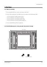
Page 111: ... avoid the following places l Do not install next to smoke and fire detectors l Do not install in an area subjected to vibration l Do not install in an area subjected to high voltage l Do not install near or around any heating apparatus 3 Use only recommended parts and components 9 2 2 Parts Wall attachment panel is sold separately Check with your dealer or Samsung Insulation holder bolt 34 61 inc...

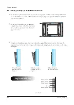
Page 112: ...el on the wall using bolts as shown in the following figure Fixing bolts must protrude from the wall appox 0 6 inches 3 Using the wall attachment panel you may adjust the angle of the display from 0 to 20 degrees The angle can be set in 5 stages with 5 degrees of distance each using the angle control holes on the sides of the pane When the angle has been set to 5 degrees When the angle has been se...

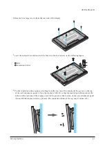
Page 113: ...on holder 6 Put the insulation rubber point protruding from the rear top of the display in the groove on the top of the wall attachment panel Lift up the display a little bit so that the insulation rubber point at the bottom of the rear side of the display is put in the groove at the bottom of the wall attachment panel Do not lift the display with any pressure The insulation rubber at the top may ...

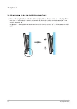
Page 114: ...ing bolts from both sides left and right of the wall attachment panel Lift and pull the bottom of the display a small amount to separate the insulation holder point from the bottom of the wall attachment panel Lift the display and separate the insulation holder point from the groove on top of the wall attachment panel Œ ...

Page 115: ...tion Drive tech that separates address pulse temporarily from sustained voltage Aging The change of operation expectancy for example operation voltage change and luminance decline related characteristics Angular distribution Characteristics which change as function of angles between perpendicularity and surface referring to dependency on angles of for example luminance or chromaticity Aperture rat...

Page 116: ...rresponding to each electric discharge In general it is defined by the shape of substrates and electrodes but can be defined by partitions Cell gap measurements identifying the gaps between substrates Cell pitch measurement that identifies the cells from the surface of substrates It varies depending on the direction of rows and columns Charge transfer curves curves expressing the quantity of elect...

Page 117: ...n or fluorescent substance chromaticity Color temperature correlated symbol CCT Seemingly temperature expressed with absolute temperature of black body radiation with the closest chro maticity This can be expressed as CCT in the form of C S McCamy CCT 437N3 3601n2 5517 n x 0 3320 0 1858 y and x y color coordinates of CIE 1931 Columm electrode Vertically successive electrodes It generally refers to...

Page 118: ...f to on Data erase pulse Wave form for data electrode that switches from on to off DC PDP Display panel whose plasma discharge is driven by direct current Decay time Time required for parameters to drop from certain level to another It can be time necessary for dropping from 90 to 10 or to e 1 level of the initial value or to certain irreversibility Dielectric layer Dielectric layer with larger su...

Page 119: ...ed color number Displayed color number Color numbers that can be made by display Dot Refer to cell pixel and subpixel The term is hard to be defined because it is not clear if the term refers to full color pixel or subpixel The term is used when referring to color related elements that make up full color pixel or subpixel Dot pitch Ambiguous expression Refer to dot cell pitch pixel pitch and subpi...

Page 120: ...olor image for example image with more than 8 bit color tone realizable display Fpc Flexible Printed Curcuit Flexible substrates with circuited copper foil on polyimide Gas mixing ratio Interchangeable terms gas mixture gas composition Gas composition within plasma device It is usually expressed with ratio of the constituent gas Gas voltage Interchangeable terms gas break down voltage Voltage wher...

Page 121: ...ass is non crystalline the word melting is not appropriate but it gets more fluid as it becomes hot Luminance Colloquial term for measurement of brightness of display It also refers to display related CIE Y constituent it is expressed by cd m2 Luminance efficacy It refers to gloss output against the total display consumption power It is calculated by the value generated through dividing gloss outp...

Page 122: ... Display that only expresses a limited color such as white green and amber Multi color display Display that can express multiple colors if not all colors Non discharge slit Refer to inter electrode gap Operating margin AC PDP voltage range that keeps cells turned on or off Generally its value gets less than memory margin because of additional factors such as temperature effect gloss ionization eff...

Page 123: ...light with atomic light release or from proper colored fluorescence substance Positive column discharge The plasma area for long glow discharge This area is a low electric field but relatively electric conductive plasma area Pre discharge Cell s state where pre discharge is taking place In this case cell s state becomes electric conductive due to formation of discharge generated by ionization proc...

Page 124: ...can pulse Waveform that injects discharge with new columns Optic defects where scratches display over certain size Seal Combining the substrates or substrate with ventilation tube Seal layer Material layer that provides the connection of substrates This can be a single layer of solder glass frit or the combination of solder glass and ring Sealing Process where free electrons that get out of the su...

Page 125: ...nergy major parts This electrode is driven by enough waveform to keep discharge of turned on state In turned off cell trigger discharge does not takes place Sustain magin The disparity between sustained voltage that keeps turned on cells and sustained voltage that can turn off cells Sustain pulse Sustained drive waveform symbol Ps Sustain vlotage Voltage level of sustained waveform Thermal compact...

Page 126: ...Releasable screen diagonal length measured between outmost pixel edges Viewrabel screen height Releasable screen height measured between outmost pixel edges Viewrable screen width Releasable screen width measured between outmost pixel edges Visible defect Imperfection that prevents displaying with proper image Wall charge Pure accumulation of positive and negative charges in cell wall Wall charge ...

Page 127: ...Samsung Electronics 10 13 Glossary Write electrode Refer to data electrode symbol Pw Write electrode Refer to data electrode symbol Vw ...

Page 128: ...10 14 Samsung Electronics MEMO ...

Page 129: ...N5505 CN5004 12P CN5002 LY1 30P CN601 13P S XF FAN 1 XF FAN 2 XF FAN 3 4 A LA03 31P LD1 4P SL BUFFER LP1 5P SX S Speaker Y CN5008 13P CN4004 12P EC2 40P FE1 40P EF1 LE02 LE01 EL1 EL2 LX1 CN4005 13P CN301 CN609 12P 6P Control CN302 3P Power S W CN601 12P CN602 9P CN606 5P Remocon CN701 31P CN1 3P CN812 CN603 4P Terminal 3P EC1 40P EC3 40P EC4 40P EC5 40P EC6 40P EC7 40P FE3 3P EF2 ...

Page 130: ...11 2 Samsung Electronics MENO ...

Page 131: ...TP11 TP12 TP10 12 Schematic Diagrams Samsung Electronics Schematic Diagrams 12 1 12 1 SCALER1 SIGNAL INPUT LVDS OUTPUT TP10 DTV PC H SYNC TP11 DTV PC V SYNC TP12 DTV PC B OUT ...

Page 132: ...ng Electronics TP04 TP05 TP03 TP02 TP06 TP07 TP06 TP07 TP05 TP04 TP07 TP09 TP08 12 2 SCALER2 VIDEO DECODER MAIN PROGRESSIVE CON TP02 Main Y IN TP03 Main C IN TP04 VS OUT TP05 HS OUT TP06 LLC1 TP07 CLK2 TP08 HOUT IVHS TP09 VOUT IVVS ...

Page 133: ...Samsung Electronics Schematic Diagrams 12 3 TP01 12 3 SCALER3 3D COMB FILTER TP01 CVBS IN ...

Page 134: ...Schematic Diagrams 12 4 Samsung Electronics 12 4 SCALER4 VIDEO DECODER PIP FIRST IN OUTPUT ...

Page 135: ...Samsung Electronics Schematic Diagrams 12 5 12 5 SCALER5 VIDEO DA CON ...

Page 136: ...chematic Diagrams 12 6 Samsung Electronics 12 6 SCALER6 VIDEO PROCESSOR SAND CASTLE PULSE GEN TP13 TP14 TP16 TP15 TP17 TP18 TP13 HS OUT TP14 VS OUT TP15 SCP H BLK TP16 SCP V BLK TP17 SCP CLAMPER TP18 SCP ...

Page 137: ...Samsung Electronics Schematic Diagrams 12 7 12 7 SCALER7 ADC VIDEO TP20 TP21 TP19 TP19 HS OUT TP20 VHS TP21 VCLK ...

Page 138: ...Schematic Diagrams 12 8 Samsung Electronics 12 8 SCALER8 ADC PC TP23 TP24 TP22 TP22 MHSYNC TP23 MHS TP24 PCLK ...

Page 139: ...Samsung Electronics Schematic Diagrams 12 9 12 9 SCALER9 PW364 TP25 TP26 TP24 TP21 TP24 PCLK TP25 MCKEXT TP26 DCKEXT TP21 VCLK ...

Page 140: ...Schematic Diagrams 12 10 Samsung Electronics 12 10 SCALER10 POWER DEGUGER MEMORY REMOCON RS232 RTC ...

Page 141: ...Samsung Electronics Schematic Diagrams 12 11 12 11 SOUND ...

Page 142: ...Schematic Diagrams 12 12 Samsung Electronics 12 12 LINE FILTER POWER SW SPEAKER TERMINAL POWER SW LINE FILTER SPEAKER TERMINAL ...

Page 143: ...Samsung Electronics Schematic Diagrams 12 13 12 13 CONTROL REMOCON CONTROL REMOCON ...

Reviews: