72
5. PCB Diagrams
5. PCB Diagrams
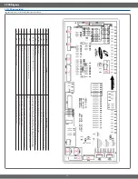
5-1 PCB Diagrams (Main)
(This Document can not be used without Samsung’s authorization)
No.
P
arts Number
Part Name
Function and Rule
1
CN01
D
oor plunger switch, cooktop warming center
, oven lamp and relay of convection fan connector
T
his is connector which is con
nected with Door plunger switch and Door lock switch. (COM-NO, COM-NC)
2
CN02
O
ven sensor Connector
This is connector which is connected with oven sensor
.
3
CN04, CN05
Relay connector
This connector is to get all operating of relay on sub PCB to be connected.
4
CN07
K
eypad Connector
This is consisted of 15 pin and take a role of getting a cable on keypad to connect with touch PCB.
5
CN08, CN09
A
T
e
rminal for connecting with SMPS Power Supply
This is to supply power with primary on Low voltage transformer
, and
AC120V with main PCB through
KDUQHVV,WZRQ¶WEHSUREOHPHYHQWKRXJK&1DQG&1KDVEHHQ
FKDQJHGZKHQ\RXLQVHUWKRXVLQJ
6
CN10
A
T
e
rminal for connecting with a small-sized RELA
Y
Power Supply
This is connector which take a role of supplying secondary voltage of Low voltage transformer with main
PCB.
7
Z
NR1
V
aristor
This is the element to protect main PCB, getting varistor to work if over voltage is supplied with varistor
.
8
IC02
DC 12V IC
This is to supply DC12V with main PCB by voltage regulator
.
9
IC03
DC 5V IC
This is to supply DC5V with main PCB by voltage regulator
.
10
CN1
1
C
ommunication with Cook-top Connector
T
his is connector which is detect operating of Cook-top

