


3 Alignments and Adjustments
3-4
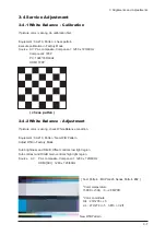
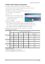
3. White Balance
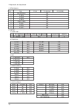
4. SVP-PX
1) ComB Filter
2) Sharpness
3) NR
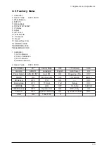
No.
Item
1
2
3
4
5
6
7
8
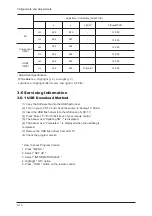
No
1
Item
Y-Filter
Range
0 ~ 255
EEPROM
NTSC
80h
PAL
SECAM
Control IC
Remark
X
H2 Gain
H4 Gain
V2 Gain
V4 Gain
Sr2 Gain
Sr4 Gain
05H
02H
0CH
04H
02H
00H
Sl2 gain
Sl4 gain
Peakth 1
Peakth 2
Peakth 3
02H
08H
04H
2FH
3FH
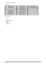
Sub-Briteness
R-offset
G-offset
B-offset
Sub-Contrast
R-Gain
G-Gain
B-Gain
TV/AV
Component
130
128
128
128
145
128
128
128
DVI (HDMI)
5) ADC Calibration
TCD3
TCD3
TCD3
TCD3
Analog
Contrast
CR
CB
Delay
Y offset
78H
20H
80H
00H
3DH
Y_NR_OFF
C_NR_OFF
Y_NR_ON
C_NR_ON
80H
4) RGB Calibration
R-offset
G-offset
B-offset
R-Gain
G-Gain
B-Gain
48H
48H
48H
39H
39H
39H
Analog
Black level
SVP Brightness
PB offset
PR offset
Y-Gain
PB-Gain
PR-Gain
80H
80H
B7H
9AH
9AH
00H
00H
Summary of Contents for LA40F71BX
Page 3: ...Contents...
Page 4: ...Contents...
Page 25: ...11 Disassembly and Reassembly 11 10 Memo...
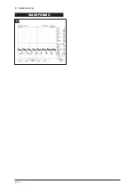
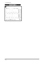
Page 29: ...4 Troubleshooting 4 4 WAVEFORMS 1...
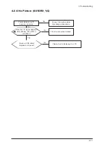
Page 31: ...4 Troubleshooting 4 6 2...
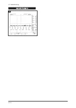
Page 33: ...4 Troubleshooting 4 8 WAVEFORMS 4 3...
Page 35: ...4 Troubleshooting 4 10 WAVEFORMS 5...
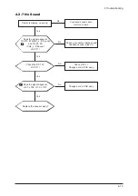
Page 37: ...4 Troubleshooting 4 12 6 WAVEFORMS...
Page 39: ...4 Troubleshooting 4 14 WAVEFORMS 7...
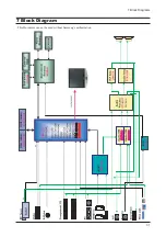
Page 51: ...7 Block Diagrams 7 2 Memo...
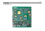
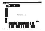
Page 52: ...12 PCB Diagram 12 1 12 PCB Diagram 12 1 Main PCB Layout 12 1 1 Main PCB Layout 40 46...
Page 53: ...12 PCB Diagram 12 2 12 1 2 Main PCB Layout 52...
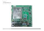
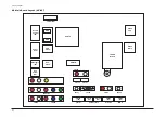
Page 54: ...12 PCB Diagram 12 3 12 2 IP Board Diagram 40...
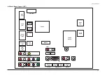
Page 55: ...12 PCB Diagram 12 4 12 3 IP BOARD Diagram 46...
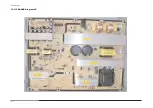
Page 56: ...8 1 8 Wiring Diagrams 8 Wiring Diagram 8 1 Wiring Diagram...
Page 69: ...8 Wiring Diagrams 8 14 Memo...
Page 146: ...13 Circuit Descriptions 13 3 13 2 Main Block...
Page 147: ...13 Circuit Descriptions 13 4 13 3 IP Board...
Page 153: ...Memo 10 Operating Instructions and Installation 10 6...
Page 161: ...14 Reference Infomation 14 8 14 3 2 Supported Modes 1...
Page 162: ...14 Reference Infomation 14 9 14 3 3 Supported Modes 2...
Page 163: ...14 Reference Infomation 14 10 14 3 4 Supported Modes 3...
Page 173: ...Memo 1 Precautions 1 4...
Page 175: ...9 Schematic Diagrams 9 2 9 2 Input Output Schematic Diagram...
Page 176: ...9 Schematic Diagrams 9 3 9 3 Input Output Schematic Diagram...
Page 177: ...9 Schematic Diagrams 9 4 9 4 Micom Schematic Diagram...
Page 178: ...9 Schematic Diagrams 9 5 9 5 SVP LX Schematic Diagram 9 5 1 SVP LX Schematic Diagram 40 46...
Page 179: ...9 Schematic Diagrams 9 6 9 5 2 SVP LX Schematic Diagram 52...
Page 180: ...9 Schematic Diagrams 9 7 9 6 Application Schematic Diagram...
Page 181: ...9 Schematic Diagrams 9 8 9 7 FRCH 100Hz LVDS Schematic Diagram...


