


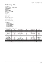
4 Troubleshooting
4-2
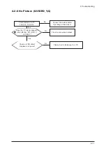
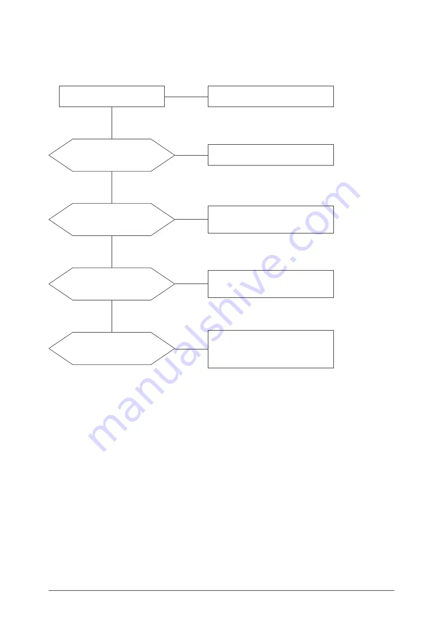
4-2-1 No Power
4-2 Checkpoints by Error Mode
Does proper DC 12V
appear at CM801?
Change a Assy PCB Power.
Yes
Yes
No
Check a connection a power cable.
No
Does proper DC A3.3V,
A5V appear at
C1034, C1032?
Check a IC109, Q113.
Change a main PCB ass'y.
Yes
No
Does proper DC 5V, 3.3V, 2.5V
1.8V appear at C1024, C1102,
C1140?
Check a IC100, IC114, IC106, IC107,
IC108. Change a main PCB ass'y
Yes
A power is supplied to set?
Check a other function.
(No picture part)
Replace a lcd panel.
No
No
LAMP off, power indicator
LED blue color?
Summary of Contents for LA40F71BX
Page 3: ...Contents...
Page 4: ...Contents...
Page 25: ...11 Disassembly and Reassembly 11 10 Memo...
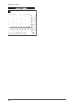
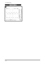
Page 29: ...4 Troubleshooting 4 4 WAVEFORMS 1...
Page 31: ...4 Troubleshooting 4 6 2...
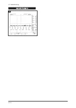
Page 33: ...4 Troubleshooting 4 8 WAVEFORMS 4 3...
Page 35: ...4 Troubleshooting 4 10 WAVEFORMS 5...
Page 37: ...4 Troubleshooting 4 12 6 WAVEFORMS...
Page 39: ...4 Troubleshooting 4 14 WAVEFORMS 7...
Page 51: ...7 Block Diagrams 7 2 Memo...
Page 52: ...12 PCB Diagram 12 1 12 PCB Diagram 12 1 Main PCB Layout 12 1 1 Main PCB Layout 40 46...
Page 53: ...12 PCB Diagram 12 2 12 1 2 Main PCB Layout 52...
Page 54: ...12 PCB Diagram 12 3 12 2 IP Board Diagram 40...
Page 55: ...12 PCB Diagram 12 4 12 3 IP BOARD Diagram 46...
Page 56: ...8 1 8 Wiring Diagrams 8 Wiring Diagram 8 1 Wiring Diagram...
Page 69: ...8 Wiring Diagrams 8 14 Memo...
Page 146: ...13 Circuit Descriptions 13 3 13 2 Main Block...
Page 147: ...13 Circuit Descriptions 13 4 13 3 IP Board...
Page 153: ...Memo 10 Operating Instructions and Installation 10 6...
Page 161: ...14 Reference Infomation 14 8 14 3 2 Supported Modes 1...
Page 162: ...14 Reference Infomation 14 9 14 3 3 Supported Modes 2...
Page 163: ...14 Reference Infomation 14 10 14 3 4 Supported Modes 3...
Page 173: ...Memo 1 Precautions 1 4...
Page 175: ...9 Schematic Diagrams 9 2 9 2 Input Output Schematic Diagram...
Page 176: ...9 Schematic Diagrams 9 3 9 3 Input Output Schematic Diagram...
Page 177: ...9 Schematic Diagrams 9 4 9 4 Micom Schematic Diagram...
Page 178: ...9 Schematic Diagrams 9 5 9 5 SVP LX Schematic Diagram 9 5 1 SVP LX Schematic Diagram 40 46...
Page 179: ...9 Schematic Diagrams 9 6 9 5 2 SVP LX Schematic Diagram 52...
Page 180: ...9 Schematic Diagrams 9 7 9 6 Application Schematic Diagram...
Page 181: ...9 Schematic Diagrams 9 8 9 7 FRCH 100Hz LVDS Schematic Diagram...


