


11 Disassembly and Reassembly
11-5
11-2 Disassembly (LA46F71BX)
Cautions : 1. Disconnect the monitor from the power source before disassembly.
2. Follow these directions carefully; never use metal instruments to pry apart the
cabinet.
Description
Picture Description
1. Place monitor face down on cushioned table.
Remove screws from the Stand.
Remove stand.
Summary of Contents for LA40F71BX
Page 3: ...Contents...
Page 4: ...Contents...
Page 25: ...11 Disassembly and Reassembly 11 10 Memo...
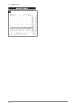
Page 29: ...4 Troubleshooting 4 4 WAVEFORMS 1...
Page 31: ...4 Troubleshooting 4 6 2...
Page 33: ...4 Troubleshooting 4 8 WAVEFORMS 4 3...
Page 35: ...4 Troubleshooting 4 10 WAVEFORMS 5...
Page 37: ...4 Troubleshooting 4 12 6 WAVEFORMS...
Page 39: ...4 Troubleshooting 4 14 WAVEFORMS 7...
Page 51: ...7 Block Diagrams 7 2 Memo...
Page 52: ...12 PCB Diagram 12 1 12 PCB Diagram 12 1 Main PCB Layout 12 1 1 Main PCB Layout 40 46...
Page 53: ...12 PCB Diagram 12 2 12 1 2 Main PCB Layout 52...
Page 54: ...12 PCB Diagram 12 3 12 2 IP Board Diagram 40...
Page 55: ...12 PCB Diagram 12 4 12 3 IP BOARD Diagram 46...
Page 56: ...8 1 8 Wiring Diagrams 8 Wiring Diagram 8 1 Wiring Diagram...
Page 69: ...8 Wiring Diagrams 8 14 Memo...
Page 146: ...13 Circuit Descriptions 13 3 13 2 Main Block...
Page 147: ...13 Circuit Descriptions 13 4 13 3 IP Board...
Page 153: ...Memo 10 Operating Instructions and Installation 10 6...
Page 161: ...14 Reference Infomation 14 8 14 3 2 Supported Modes 1...
Page 162: ...14 Reference Infomation 14 9 14 3 3 Supported Modes 2...
Page 163: ...14 Reference Infomation 14 10 14 3 4 Supported Modes 3...
Page 173: ...Memo 1 Precautions 1 4...
Page 175: ...9 Schematic Diagrams 9 2 9 2 Input Output Schematic Diagram...
Page 176: ...9 Schematic Diagrams 9 3 9 3 Input Output Schematic Diagram...
Page 177: ...9 Schematic Diagrams 9 4 9 4 Micom Schematic Diagram...
Page 178: ...9 Schematic Diagrams 9 5 9 5 SVP LX Schematic Diagram 9 5 1 SVP LX Schematic Diagram 40 46...
Page 179: ...9 Schematic Diagrams 9 6 9 5 2 SVP LX Schematic Diagram 52...
Page 180: ...9 Schematic Diagrams 9 7 9 6 Application Schematic Diagram...
Page 181: ...9 Schematic Diagrams 9 8 9 7 FRCH 100Hz LVDS Schematic Diagram...


