


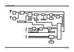
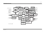

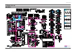
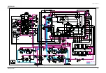

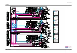

Block Diagram
7-2
Samsung Electronics
7-2 Main Block Diagram
TUNER 2
CABLE
3D-Comb
uPD6488
Chroma
TDA9141
A/V
Switch
TA8851AN
EXT. A/V INPUT
Video:3, S-video : 3
R.G.B
Interface CXA2011Q
R,G,B Controller
CXA1839Q
IF
Module
ADC,DAC
and VOLCONT
CS4226
VOL Ctrl
SSM2160
NT Caption
Z86129
TUNER 1
HD/NT
Switch
LA7220
EXT. Y/P B/PR
CTI
TDA4566
Panorama
TC90A18
Digital Board
IF
IF
Digital Baseband Signal
CVBS/L/R
CVBS/L/R
or
Y/C/L/R
CVBS
Y/C
Y/C
Caption Data
R/G/B
Ntsc Vchip Data
Y/U/V
Y/U/V
Switch
LA7220
Y/U/V
Y/U/V
Y
U/V
U/V
L/R
Serial Data
Audio Data 0/1/2
L/R/C/LS/RS/W
Tone Ctrl
TDA8425
L/R
L
R
C
LS/RS/W
TO
AMP BOARD
TO OUTPUT JACK
Digital Audio Out
External Digital Audio IN
R/G/B
2H/2V
SYNC
Y/U/V
R/G/B
TO
CRT BOARD
R
G
B
Summary of Contents for HCH551WX
Page 2: ...ELECTRONICS Samsung Electronics Co Ltd NOV 1998 Printed in Korea 3APT52A 5501 ...
Page 23: ...MEMO 3 16 Samsung Electronics ...
Page 62: ...8 2 Samsung Electronics MEMO ...
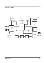
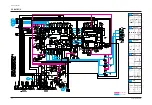
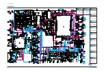
Page 67: ...Schematic Diagrams Samsung Electronics 9 5 9 5 3DCOMB1 Power Line Signal Line ...
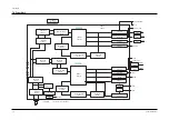
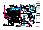
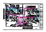
Page 68: ...Schematic Diagrams 9 6 Samsung Electronics 9 6 IF_MODULE Power Line Signal Line ...
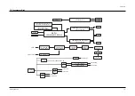
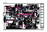
Page 73: ...Schematic Diagrams Samsung Electronics 9 11 9 11 CONTROL SUB Power Line ...


