


1 Precautions
1-2
1-2-1 General Servicing
Precautions
1.
Always unplug the unit s AC power cord from the AC
power source and disconnect the DC Power Jack
before attempting to:
(a) remove or reinstall any component or assembly, (b)
disconnect PCB plugs or connectors, (c) connect a test
component in parallel with an electrolytic capacitor.
2.
Some components are raised above the printed circuit
board for safety. An insulation tube or tape is
sometimes used. The internal wiring is sometimes
clamped to prevent contact with thermally hot
components. Reinstall all such elements to their
original position.
3. After servicing, always check that the screws,
components and wiring have been correctly
reinstalled. Make sure that the area around the
serviced part has not been damaged.
1.
Immediately before handling any semiconductor
components or assemblies, drain the electrostatic
charge from your body by touching a known earth
ground. Alternatively, wear a discharging wrist-strap
device. To avoid a shock hazard, be sure to remove the
wrist strap before applying power to the monitor.
2.
After removing an ESD-equipped assembly, place it
on a conductive surface such as aluminum foil to
prevent accumulation of an electrostatic charge.
3.
Do not use freon-propelled chemicals. These can
generate electrical charges sufficient to damage ESDs.
4.
Use only a grounded-tip soldering iron to solder or
desolder ESDs.
5.
Use only an anti-static solder removal device. Some
solder removal devices not classified as anti-static
can generate electrical charges sufficient to damage
ESDs.
4.
Check the insulation between the blades of the AC
plug and accessible conductive parts (examples: metal
panels, input terminals and earphone jacks).
5.
Insulation Checking Procedure: Disconnect the power
cord from the AC source and turn the power switch
ON. Connect an insulation resistance meter (500 V) to
the blades of the AC plug.
The insulation resistance between each blade of the
AC plug and accessible conductive parts (see above)
should be greater than 1 megohm.
6.
Always connect a test instrument s ground lead to the
instrument chassis ground before connecting the
positive lead; always remove the instrument s ground
lead last.
6.
Do not remove a replacement ESD from its protective
package until you are ready to install it. Most
replacement ESDs are packaged with leads that are
electrically shorted together by conductive foam,
aluminum foil or other conductive materials.
7.
Immediately before removing the protective material
from the leads of a replacement ESD, touch the
protective material to the chassis or circuit assembly
into which the device will be installed.
Caution: Be sure no power is applied to
the chassis or circuit and
observe all other safety
precautions.
8.
Minimize body motions when handling unpackaged
replacement ESDs. Motions such as brushing clothes
together, or lifting your foot from a carpeted floor can
generate enough static electricity to damage an ESD.
1-3 Static Electricity Precautions
Some semiconductor (solid state) devices can be easily damaged by static electricity. Such components are commonly called
Electrostatically Sensitive Devices (ESD). Examples of typical ESD are integrated circuits and some field-effect transistors.
The following techniques will reduce the incidence of component damage caused by static electricity.
1-2 Servicing Precautions
WARNING:
An electrolytic capacitor installed with the wrong polarity might explode.
Caution:
Before servicing units covered by this service manual, read and follow the Safety
Precautions section of this manual.
Note:
If unforeseen circumstances create conflict between the following servicing precautions and any of the safety
precautions, always follow the safety precautions.
Summary of Contents for GBD26KS
Page 2: ... 豪华超薄设计 超级画质 超级音质 极其舒适 使用方便 ...
Page 7: ...Memo 1 Precautions 1 4 ...
Page 11: ... _ _ _ _ ab ab ab ab c c c c IJ Id MN U ...
Page 22: ... ...
Page 23: ... 0 1234453 6789 AB CDEF GHIJ GK GK GK GK GLCM 1NOPQ RSTUV WXYZ LC YZ 23 _ ...
Page 27: ... F F F F º D D D D wx ny gh t t t I 0 9 0 9 B EF EF CDEF 4 4 PQ PQ PQ PQ L ...
Page 28: ... L L 6 À Á cd 8 8 8 à 8 8 8 ...
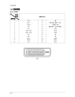
Page 30: ...10 2 Connection Panel 10 Operating Instructions and Installation 10 2 ...
Page 35: ... 0123 45 6789 ABCDEFGHI JIK LM N O PQR LST O PQR ...
Page 36: ... UVMNW OST LSTXY OQR WUVSTXY ...
Page 37: ... LZI O LZI OQR WUVZI ...
Page 38: ... L OQR LAZXY OQR UVAZXY ...
Page 39: ... UV _AZ ab ...
Page 40: ... ...
Page 44: ... ...
Page 45: ... ...
Page 46: ... ...
Page 47: ... ...
Page 48: ... ...
Page 51: ... g Þ Õ Ì W L N0 õö k kü ...
Page 52: ... y UV e J V y h e G y UV h e ...
Page 55: ...13 Circuit Descriptions 13 3 13 2 Main Block ...
Page 56: ...13 Circuit Descriptions 13 4 13 3 SMPS Board 13 3 1 26 32 SMPS Block 13 3 2 26 32 SMPS Block ...
Page 57: ...13 Circuit Descriptions 13 5 13 3 3 26 32 SMPS Block 13 3 4 26 32 SMPS Block ...
Page 58: ...13 Circuit Descriptions 13 6 ...
Page 59: ...13 Circuit Descriptions 13 7 13 3 5 32 40 IP Board 13 3 6 32 40 IP Board ...
Page 60: ...Memo 13 Circuit Descriptions 13 8 ...
Page 61: ... ...
Page 62: ... 0 1 0 1 0 1 2345 1 ...
Page 63: ... 67 89 ABC D EFG6 H I 1 8 JKJL1 ...
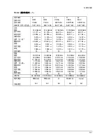
Page 64: ...4 Troubleshooting 4 4 WAVEFORMS 1 R G B Output Signal of IC500 ...
Page 65: ... 67 89 ABC D EFG6 H JKJ L1 8 M JKJL1 ...
Page 66: ...4 Troubleshooting 4 6 2 Digital Output Data of IC500 3 Signal of HDMI Data ...
Page 67: ... 67 N OPQ ABC D EFG6 H 1 1 8 M JKJL1 RS I RS ...
Page 68: ...4 Troubleshooting 4 8 WAVEFORMS 4 Tuner_CVBS Output Signal 3 CVBS Output Signal ...
Page 69: ... 67 TU V ABC D EFG6 H 1 8 M JKJL1 WS ...
Page 70: ...4 Troubleshooting 4 10 WAVEFORMS 4 CVBS Output Signal ...
Page 71: ... 67 V ABC D EFG6 H 1 8 M JKJL 1 XYZ 4 ...
Page 72: ...4 Troubleshooting 4 12 2 Digital Output Data of IC500 5 Analog Signal Y C to IC500 WAVEFORMS ...
Page 73: ... TU N OPQ 1 1 _ Q RS I RS ...
Page 74: ...4 Troubleshooting 4 14 WAVEFORMS 6 The Signal are Inputed to IC603 7 DC 12V ...
Page 150: ...7 Block Diagrams 7 2 Memo ...
Page 151: ...12 PCB Diagram 12 1 12 PCB Diagram 12 1 26 Main PCB Diagram ...
Page 153: ...12 PCB Diagram 12 3 12 3 26 SMPS board ...
Page 154: ...12 PCB Diagram 12 4 12 4 32 SMPS board ...
Page 155: ...12 PCB Diagram 12 5 12 5 40 IP Board ...
Page 156: ...12 PCB Diagram 12 6 Memo ...
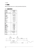
Page 157: ...8 1 8 Wiring Diagrams 8 Wiring Diagram 8 1 LA26R71B LA32R71B LA40R71B Wiring Diagram ...
Page 158: ...8 Wiring Diagrams 8 2 8 2 Main Board Layout ...
Page 161: ...8 5 8 Wiring Diagrams ...
Page 162: ...8 Wiring Diagrams 8 6 8 4 Power Board Layout ...
Page 165: ...8 9 8 Wiring Diagrams ...
Page 168: ...8 Wiring Diagrams 8 12 Memo ...
Page 169: ... ...
Page 170: ... ...
Page 171: ... ...
Page 172: ... ...
Page 173: ... ...
Page 174: ... ...
Page 175: ... 01 23 45 6 78 9 A BC DE FGH I ...


