
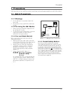


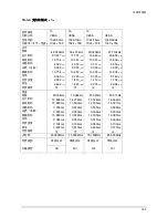
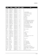


!"#
$
%
%
%
%
!"#
"
&
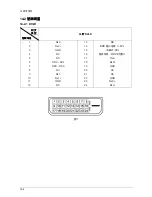
'()*+',(-.//-0/12-0/.+'33
"
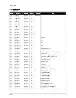
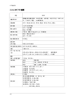
*+',452%
*+',452%6-0/,78-+*+9'452 9:;<&=<'*8*+',452%
3'><
*+',<)25?@452/-0/12-0/.+'3354A
',, )25@@8'9/*+-9*,58)*.-1,'
A+*225(1'B',
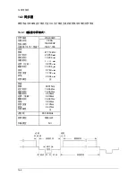
%
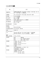
*+',452A-:'%
,-8:'3-0+C
1-.3$@@@452>
*+',452A%
*225(=3,-8:'3-0+A%85:'
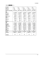
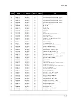
")*+',
")*+',
")*+',
$
")*+',
")*+',
")*+',
")*+',
%
")*+',
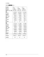
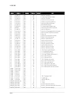
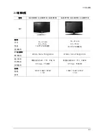
5,529552:-+*.'39/*+0'452%
>AC6
&
5,52552:-+*.'39/*+0'95:'8*+*0'8'+.
"
5,52552:-+*.'3/*+0'*+',5:'
Summary of Contents for GBD26KS
Page 2: ... 豪华超薄设计 超级画质 超级音质 极其舒适 使用方便 ...
Page 7: ...Memo 1 Precautions 1 4 ...
Page 11: ... _ _ _ _ ab ab ab ab c c c c IJ Id MN U ...
Page 22: ... ...
Page 23: ... 0 1234453 6789 AB CDEF GHIJ GK GK GK GK GLCM 1NOPQ RSTUV WXYZ LC YZ 23 _ ...
Page 27: ... F F F F º D D D D wx ny gh t t t I 0 9 0 9 B EF EF CDEF 4 4 PQ PQ PQ PQ L ...
Page 28: ... L L 6 À Á cd 8 8 8 à 8 8 8 ...
Page 30: ...10 2 Connection Panel 10 Operating Instructions and Installation 10 2 ...
Page 35: ... 0123 45 6789 ABCDEFGHI JIK LM N O PQR LST O PQR ...
Page 36: ... UVMNW OST LSTXY OQR WUVSTXY ...
Page 37: ... LZI O LZI OQR WUVZI ...
Page 38: ... L OQR LAZXY OQR UVAZXY ...
Page 39: ... UV _AZ ab ...
Page 40: ... ...
Page 44: ... ...
Page 45: ... ...
Page 46: ... ...
Page 47: ... ...
Page 48: ... ...
Page 51: ... g Þ Õ Ì W L N0 õö k kü ...
Page 52: ... y UV e J V y h e G y UV h e ...
Page 55: ...13 Circuit Descriptions 13 3 13 2 Main Block ...
Page 56: ...13 Circuit Descriptions 13 4 13 3 SMPS Board 13 3 1 26 32 SMPS Block 13 3 2 26 32 SMPS Block ...
Page 57: ...13 Circuit Descriptions 13 5 13 3 3 26 32 SMPS Block 13 3 4 26 32 SMPS Block ...
Page 58: ...13 Circuit Descriptions 13 6 ...
Page 59: ...13 Circuit Descriptions 13 7 13 3 5 32 40 IP Board 13 3 6 32 40 IP Board ...
Page 60: ...Memo 13 Circuit Descriptions 13 8 ...
Page 61: ... ...
Page 62: ... 0 1 0 1 0 1 2345 1 ...
Page 63: ... 67 89 ABC D EFG6 H I 1 8 JKJL1 ...
Page 64: ...4 Troubleshooting 4 4 WAVEFORMS 1 R G B Output Signal of IC500 ...
Page 65: ... 67 89 ABC D EFG6 H JKJ L1 8 M JKJL1 ...
Page 66: ...4 Troubleshooting 4 6 2 Digital Output Data of IC500 3 Signal of HDMI Data ...
Page 67: ... 67 N OPQ ABC D EFG6 H 1 1 8 M JKJL1 RS I RS ...
Page 68: ...4 Troubleshooting 4 8 WAVEFORMS 4 Tuner_CVBS Output Signal 3 CVBS Output Signal ...
Page 69: ... 67 TU V ABC D EFG6 H 1 8 M JKJL1 WS ...
Page 70: ...4 Troubleshooting 4 10 WAVEFORMS 4 CVBS Output Signal ...
Page 71: ... 67 V ABC D EFG6 H 1 8 M JKJL 1 XYZ 4 ...
Page 72: ...4 Troubleshooting 4 12 2 Digital Output Data of IC500 5 Analog Signal Y C to IC500 WAVEFORMS ...
Page 73: ... TU N OPQ 1 1 _ Q RS I RS ...
Page 74: ...4 Troubleshooting 4 14 WAVEFORMS 6 The Signal are Inputed to IC603 7 DC 12V ...
Page 150: ...7 Block Diagrams 7 2 Memo ...
Page 151: ...12 PCB Diagram 12 1 12 PCB Diagram 12 1 26 Main PCB Diagram ...
Page 153: ...12 PCB Diagram 12 3 12 3 26 SMPS board ...
Page 154: ...12 PCB Diagram 12 4 12 4 32 SMPS board ...
Page 155: ...12 PCB Diagram 12 5 12 5 40 IP Board ...
Page 156: ...12 PCB Diagram 12 6 Memo ...
Page 157: ...8 1 8 Wiring Diagrams 8 Wiring Diagram 8 1 LA26R71B LA32R71B LA40R71B Wiring Diagram ...
Page 158: ...8 Wiring Diagrams 8 2 8 2 Main Board Layout ...
Page 161: ...8 5 8 Wiring Diagrams ...
Page 162: ...8 Wiring Diagrams 8 6 8 4 Power Board Layout ...
Page 165: ...8 9 8 Wiring Diagrams ...
Page 168: ...8 Wiring Diagrams 8 12 Memo ...
Page 169: ... ...
Page 170: ... ...
Page 171: ... ...
Page 172: ... ...
Page 173: ... ...
Page 174: ... ...
Page 175: ... 01 23 45 6 78 9 A BC DE FGH I ...


