background image

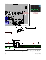
Trouble Shooting

4-0

Samsung Electronics

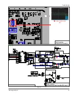
Fig. 4-0

AIC8

PIC5

AIC3

Refer to a pattern 

image of Main PCB page 6-4

CVBS(Color-bar)

Pin (VC , VR6)

Refer to a pattern 

image of Analog Audio/Video (Main PCB) Page 7-6

Summary of Contents for BDP1500 - Blu-Ray Disc Player

Page 1: ... under applicable International and or domestic law Chassis Blu Ray BASIC BD P1500 Application Model BD P1500 Application Area XAA XAC AFS XAX XAZ STR If you want to know additional information which is not includ ed on this Service Manual Please refer to the SKP Samsung Knowledge Portal web site Area Web Site North America URL http service samsungportal com Latin America URL http latin samsungpor...

Page 2: ... 8 6 1 Wiring Diagram 6 2 6 2 Main PCB 6 3 6 3 S M P S PCB 6 5 6 4 Front key PCB 6 7 6 5 Power Key PCB 6 8 7 Schematic Diagrams 7 1 7 22 7 1 All block Diagram 7 2 7 2 Power 7 3 7 3 S M P S S M P S PCB 7 5 7 4 Analog Audio Video Main PCB 7 6 7 5 HDMI CEC Main PCB 7 8 7 6 HDMI Transmitter Main PCB 7 9 7 7 7440 Boot Strap Option Main PCB 7 10 7 8 7440 EBI ADDR EBI DATA Main PCB 7 11 7 9 7440 Clocks B...

Page 3: ... a metering system that complies with American National Standardsp institute ANSI C101 1 Leakage Current for Appliances and Underwriters Laboratories UL 1270 40 7 With the instrument s AC switch first in the ON position and then in the OFF position measure from a known earth ground metal water pipe conduit etc to all exposed metal parts of the instrument antennas handle brackets metal cabinets scr...

Page 4: ...ched out of place or frayed wiring Do not change spacing between a component and the printed circuit board Check the AC power cord for damage 5 Components parts and or wiring that appear to have overheated or that are otherwise damaged should be replaced with components parts and or wiring that meet original specifications Additionally determine the cause of overheating and or damage and if necess...

Page 5: ...nd lead last 2 The service precautions are indicated or printed on the cabinet chassis or components When servicing follow the printed or indicated service precautions and service materials 3 The components used in the unit have a specified flame resistance and dielectric strength When replacing components use components which have the same ratings Components identified by shading by or by in the ...

Page 6: ...bly 3 Use only a grounded tip soldering iron to solder or unsolder ESD devices 4 Use only an anti static solder removal devices Some solder removal devices not classified as anti static can generate electrical charges suffi cient to damage ESD devices 5 Do not use freon propelled chemicals These can generate electrical charges sufficient to damage ESD devices 6 Do not remove a replacement ESD devi...

Page 7: ...our hands on the conductive sheet This gives them the same ground as the sheet 4 Remove the optical pick up block 5 Perform work on top of the conductive sheet Be careful not to let your clothes or any other static sources to touch the unit u Be sure to put on a wrist strap grounded to the sheet u Be sure to lay a conductive sheet made of copper etc Which is grounded to the table 6 Short the short...

Page 8: ...Precautions 1 Samsung Electronics M E M O ...

Page 9: ...Speed 4 8 5 6 m sec Maximum Play Time 20 min Video Output Composite Video 1 channel 1 0 Vp p 75 Ω load Blu ray Disc 480i DVD 480i Component Video Y 1 0 Vp p 75 Ω load Pr 0 70 Vp p 75 Ω load Pb 0 70 Vp p 75 Ω load Blu ray Disc 1080i 720p 480p 480i DVD 480p 480i S Video Luminance Signal 1 0 Vp p 75 Ω load Chrominance Signal 0 3 Vp p 75 Ω load Blu ray Disc 480i DVD 480i Video Audio HDMI 480p 720p 108...

Page 10: ... x 720 HD q For High Definition Playback To view high definition contents in BD discs an HDTV High Definition Television is required Some discs may require using the player s HDMI OUT to view high Definition content The ability to view high Definition content on BD discs may be limited depending on the resolution of your TV q Graphic planes Two individual full HD resolution 1920x1080 video layers ...

Page 11: ...y images When switching from the fi rst layer to the second layer of a dual layered DVD Video disc there may be momentary distortion in the image and sound This is not a malfunction of the unit Once a DVD RW R recorded in Video Mode is fi nalized it becomes DVD Video Pre recorded prestamped commercial DVDs with movies are also referred to as DVD Videos This unit can play back pre recorded commerci...

Page 12: ...egion Number for this Blu ray disc player is described on the rear panel of the Blu ray disc player Disc Type Blu ray DVD Video Region code BD Region Code Area A North America Central America South America Korea Japan Taiwan Hong Kong and South East Asia B Europe Greenland French territories Middle East Africa Australia and New Zealand C India China Russia Central and South Asia 2 1 6 Blu ray Disc...

Page 13: ...10bit 10bit 10bit Audio DAC 24bit 192kHz 24bit 192kHz 24bit 192kHz Loader BD ROM O O O BD RE BD R O X O DVD RAM O X X DVD RW O O O DVD ROM O O O DVD R O O O DVD R X X X DVD RW X X X CD ROM O O O CD R O O O CD RW O O O A V Play able Media BD ROM O O O BD RE BD R O X O DVD Video O O O DVD Audio X X X DVD VR O X X Not finalized DVD V Mode X X X VCD 1 1 2 0 X X X SVCD CVD X X X CD DA O O O DTS CD O O ...

Page 14: ...rk Remote Control AK59 00070D Model Standard of BD P1500 XAA Batteries for Remote Control 4301 001035 Model Standard of BD P1500 XAA S N A Instruction Manual AK68 01608A Model Standard of BD P1500 XAA Quick Guide AK68 01610A Model Standard of BD P1500 XAA S N A Component Cable AC39 42001R Model Standard of BD P1500 XAA ...

Page 15: ... PCB Samsung Electronics 3 3 1 1 Top Cabinet Removal 1 Remove 5 Screws q w 2 Lift up the Top Cabinet e in direction of arrow Fig 3 1 Top Cabinet Removal q 3 SCREWS 3X10 B e TOP CABINET CAUTION Connector Must be remove with care w 2 SCREWS 3X10 B ...

Page 16: ...d Reassembly 3 Samsung Electronics 3 1 2 Ass y Front Cabinet Removal 1 Release 7 Hooks q w e r and Ass y Front Cabinet t Fig 3 2 Ass y Front Cabinet Removal w 1 HOOK t ASS Y FRONT CABINET r 2 HOOKS e 3 HOOKS q 1 HOOK ...

Page 17: ...Samsung Electronics 3 Disassembly and Reassembly 3 1 3 Ass y Deck Removal 1 Remove 4 Screws q from the Ass y Deck w and lift it up Fig 3 3 Ass y Deck Removal q 4 SCREWS 3X10 W w ASS Y DECK ...

Page 18: ...Disassembly and Reassembly 3 Samsung Electronics 3 1 4 S M P S PCB Removal 1 Remove 3 Screws q from the S M P S PCB w and lift it up Fig 3 4 S M P S PCB Removal q 3 SCREWS 3X8 W w S M P S PCB ...

Page 19: ...Samsung Electronics 3 Disassembly and Reassembly 3 1 5 Main PCB Removal 1 Remove 7 Screws q wfrom the Main PCB e and lift it up Fig 3 5 Main PCB Removal e MAIN PCB q 4 SCREWS 3X8 W w 3 SCREWS 3X10 B ...

Page 20: ...Disassembly and Reassembly 3 Samsung Electronics 3 2 PCB Location Fig 3 6 PCB Location MAIN PCB S M P S PCB ...

Page 21: ...4 Trouble Shooting Samsung Electronics 4 4 1 Trouble Shooting 4 2 4 2 Software Update 4 21 ...

Page 22: ...ormal C1S05 voltage is normal voltage Switching operation of IC1S10 is normal Change the SMPS PCB Change fuse Change BD1 Change IC1S10 No Yes No No Refer to a pattern image of Table 4 1 Yes Yes Refer to a pattern image of Table 4 1 Refer to a pattern image of Table 4 1 Refer to a pattern image of Table 4 1 ...

Page 23: ...Samsung Electronics 4 Trouble Shooting Fig 4 1 Refer to a pattern image of S M P S Page 7 5 Refer to a pattern image of S M P S PCB page 6 5 ...

Page 24: ... Check Current Digital Audio Setting is PCM Set to Bitstream No Yes Check the A V Receiver can Decode Current Bit Steam No Yes check the jack IC98 soldering or replace IC98 Check the Audio Data at AR160 No Yes Replace the Main PCB Refer to a pattern image of Table 4 2 ...

Page 25: ...ctronics 4 Trouble Shooting Digital Audio Analog Audio Analog Video Fig 4 2 Refer to a pattern image of Analog Audio Video Main PCB Page 7 6 Refer to a pattern image of Main PCB page 6 3 q DIGITAL AUDIO DATA AR160 ...

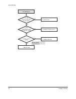
Page 26: ... of AIC8 PIN3 5 7 Clock data PIN6 Audio data Check the Audio signal at PIN 20 21 22 23 of AIC8 Check the Audio signal at AIC3 Audio cable error Replace the main PCB Check AIC2 soldering or replace AIC2 Check AIC3 soldering of peripheral devices No Yes No No Yes Yes Refer to a pattern image of Table 4 3 ...

Page 27: ... Electronics 4 Trouble Shooting Audio Analog Video Fig 4 3 AIC8 PIC5 AIC3 Refer to a pattern image of Main PCB page 6 4 q ANALOG AUDIO DATA AIC3 Refer to a pattern image of Analog Audio Video Main PCB Page 7 6 ...

Page 28: ... the deck power at LCON1 D3 3V D5V D12V Is the STAT cable between main deck inserted correctly Check the clock at X1 25MHz Change the deck Check the power Reinsert SATA Cable correctly Change the Main board No Yes No No Yes Yes Refer to a pattern image of Table 4 4 ...

Page 29: ...Samsung Electronics 4 Trouble Shooting Fig 4 4 Refer to a pattern image of Main PCB page 6 3 Refer to a pattern image of Ethernet USB S ATA P ATA Main PCB Page 7 15 25MHz ...

Page 30: ...on battery OK Is the FFC cable between Front panel Main OK FU3 PIN3 SIGNAL OK Check the Power of FIC1 PIN9 or change the Main PCB Change the battery Re insert FFC cable correctly Check FU3 or change the Front panel PCB No Yes No No Yes Yes Refer to a pattern image of Table 4 5 ...

Page 31: ...Samsung Electronics 4 11 Trouble Shooting Fig 4 5 Refer to a pattern image of Front Key Front PCB Page 7 20 Refer to a pattern image of Front keyPCB page 6 7 q Remote control eye data FU3 Pin3 ...

Page 32: ...uble Shooting 4 12 Samsung Electronics No Picture Logo screen is OK NO LOGO HDMI No Yes HDMI No Yes BD DVD Playback is OK No Yes CHANGE THE MAIN PCB NO LOGO Component Component No Yes NO LOGO CVBS S Video ...

Page 33: ...le error Check the Video select cable connection TV mode Check U1 power input Y1 oscillation Memory interface Check HCN1 Connector and HDMI cable connection No Yes No No Yes Yes Refer to a pattern image of Table 4 6 data output from HIC1 pin30 31 33 34 36 37 39 40 Check the HIC1 power input and peripheral devices No Yes Refer to a pattern image of Table 4 7 Refer to a pattern image of Table 4 6 ...

Page 34: ...oting 4 14 Samsung Electronics C15 Refer to a pattern image of Main PCB page 6 3 q Digital Video signal U1 HRN3 HRN8 w Y1 _CLOCK SIGNAL 54MHz Fig 4 6 Refer to a pattern image of HDMI Transmitter Main PCB Page 7 9 ...

Page 35: ...g Electronics 4 15 Trouble Shooting HIC1 Refer to a pattern image of Main PCB page 6 3 Fig 4 7 q HDMI OUTPUT DATA HIC1 pin30 31 33 34 36 37 39 40 Refer to a pattern image of HDMI Transmitter Main PCB Page 7 9 ...

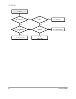
Page 36: ...n and TV mode Video output from U1 VC6 1 4 Video output from VIC1 VR12 13 14 Component cable error Check the Video select cable connection TV mode U1 soldering error Check VIC1 soldering of peripheral devices No Yes No No Yes Yes Refer to a pattern image of Table 4 8 Refer to a pattern image of Table 4 9 ...

Page 37: ... Audio Analog Audio Analog Video Fig 4 8 AIC8 PIC5 AIC3 Refer to a pattern image of Main PCB page 6 4 w Pb Color bar Pin U1 VR1 q Y Color bar Pin U1 VR6 e Pr Color bar Pin U1 VR4 Refer to a pattern image of Analog Audio Video Main PCB Page 7 6 ...

Page 38: ...Samsung Electronics Fig 4 9 AIC8 PIC5 AIC3 Refer to a pattern image of Main PCB page 6 4 q Y Color bar Pin VR12 e Pr Color bar Pin VR14 w Pb Color bar Pin VR13 Refer to a pattern image of Analog Audio Video Main PCB Page 7 6 ...

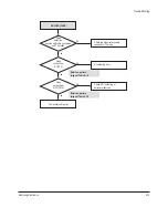
Page 39: ...ion and TV mode Video output from U1 VC3 Video output from VIC1 VR16 Component cable error Check the Video select cable connection TV mode U1 soldering error Check VIC1 soldering of peripheral devices No Yes No No Yes Yes Refer to a pattern image of Table 4 10 Refer to a pattern image of Table 4 10 ...

Page 40: ...uble Shooting 4 20 Samsung Electronics Fig 4 10 AIC8 PIC5 AIC3 Refer to a pattern image of Main PCB page 6 4 q CVBS Color bar Pin VC 3 VR16 Refer to a pattern image of Analog Audio Video Main PCB Page 7 6 ...

Page 41: ...e 1 Insert update CD and close the tray 4 2 1 Main F W Update Method Fig 4 11 Fig 4 12 Fig 4 13 2 Tray opened automatically then Press YES if the up date CD you insert is a later one than before 3 Wait about 7 minutes 4 When finished power goes off automatically ...

Page 42: ...close the tray 2 Tray opened automatically then Press YES if the up date CD you insert is a later one than before 4 2 2 Loader F W Update Method for Disc Physical Problem Fig 4 14 Fig 4 15 Fig 4 16 3 Wait about 1 2 minutes 4 When finished power goes off automatically ...

Page 43: ...5 Exploded View and Parts List 삼성전자 5 5 1 Cabinet Assembly 5 2 5 2 Electrical Parts List 5 4 ...

Page 44: ...s and Parts List 5 This Document can not be used without Samsung s authorization Samsung Electronics 5 1 Cabinet Assembly P025 W001 W001 W001 W001 W009 P001 P003 H003 P007P P007F C001 A001 W009 C015A W200 W200 W200 ...

Page 45: ...BD P1500 ASSY 1 SA H003 AK97 02218A ASSY BDP LOADER NEC BD P1500 ASSY 1 SA P001 AK92 01649A ASSY PCB MAIN BD P1500 XAA ASSY PCB 1 SA P003 AK92 01655A ASSY PCB SMPS BD P1500 XAA ASSY PCB 1 SA P007F AK92 01650A ASSY PCB FRONT KEY BD P1500 XAA ASS 1 SA P007P AK92 01651A ASSY PCB POWER KEY BD P1500 XAA ASS 1 SA P025 AC39 10200N CBF POWER CORD AT US EP2 Y HOUSING 1 SA W001 6003 000275 SCREW TAPTITE BH ...

Page 46: ... TP 1608 1 SA AR24 2007 000120 R CHIP 680ohm 5 1 10W TP 1608 1 SA AR25 2007 000120 R CHIP 680ohm 5 1 10W TP 1608 1 SA AR26 2007 000070 R CHIP 0ohm 5 1 10W TP 1608 1 SA AR27 2007 000208 R CHIP 1 1Kohm 1 1 10W TP 1608 1 SA AR28 2007 000683 R CHIP 3 3Kohm 1 1 10W TP 1608 1 SA AR30 2007 000040 R CHIP 150ohm 1 1 10W TP 1608 1 SA AR31 2007 000040 R CHIP 150ohm 1 1 10W TP 1608 1 SA AR40 2007 000512 R CHI...

Page 47: ...TP 1608 1 SA C80 2203 006048 C CER CHIP 100nF 10 10V X7R 1005 1 SA C85 2203 006474 C CER CHIP 22000nF 20 6 3V X5R 201 1 SA C86 2203 006474 C CER CHIP 22000nF 20 6 3V X5R 201 1 SA C87 2203 006474 C CER CHIP 22000nF 20 6 3V X5R 201 1 SA C88 2203 006474 C CER CHIP 22000nF 20 6 3V X5R 201 1 SA C89 2203 006474 C CER CHIP 22000nF 20 6 3V X5R 201 1 SA C90 2203 006474 C CER CHIP 22000nF 20 6 3V X5R 201 1 ...

Page 48: ...IP 100ohm 5 1 10W TP 1608 1 SA HR30 2007 000084 R CHIP 4 7Kohm 5 1 10W TP 1608 1 SA HR31 2007 000084 R CHIP 4 7Kohm 5 1 10W TP 1608 1 SA HR33 2007 000962 R CHIP 5 1Kohm 1 1 10W TP 1608 1 SA HR34 2007 000070 R CHIP 0ohm 5 1 10W TP 1608 1 SA HR36 2007 000070 R CHIP 0ohm 5 1 10W TP 1608 1 SA HR4 2007 008107 R CHIP 698ohm 1 1 10W TP 1608 1 SA HR5 2007 000074 R CHIP 100ohm 5 1 10W TP 1608 1 SA HR6 2007...

Page 49: ...CHIP 0 1nF 5 50V C0G 1608 1 SA PC48 2203 000888 C CER CHIP 4 7nF 10 50V X7R 1608 1 SA PC5 2203 005148 C CER CHIP 100nF 10 16V X7R TP 160 1 SA PC51 2203 005148 C CER CHIP 100nF 10 16V X7R TP 160 1 SA PC52 2203 005148 C CER CHIP 100nF 10 16V X7R TP 160 1 SA PC53 2203 005148 C CER CHIP 100nF 10 16V X7R TP 160 1 SA PC54 2203 005148 C CER CHIP 100nF 10 16V X7R TP 160 1 SA PC55 2203 005148 C CER CHIP 10...

Page 50: ...0 R CHIP 10Kohm 5 1 10W TP 1608 1 SA R189 2007 000090 R CHIP 10Kohm 5 1 10W TP 1608 1 SA R19 2007 000084 R CHIP 4 7Kohm 5 1 10W TP 1608 1 SA R190 2007 000090 R CHIP 10Kohm 5 1 10W TP 1608 1 SA R191 2007 000090 R CHIP 10Kohm 5 1 10W TP 1608 1 SA R192 2007 000090 R CHIP 10Kohm 5 1 10W TP 1608 1 SA R197 2007 000090 R CHIP 10Kohm 5 1 10W TP 1608 1 SA R198 2007 000090 R CHIP 10Kohm 5 1 10W TP 1608 1 SA...

Page 51: ...007 000123 R CHIP 1 5Kohm 5 1 10W TP 1608 1 SA scon1 3711 006512 CONNECTOR HEADER 1WALL 7P 1R 1 27mm 1 SA U1 1204 002900 IC VIDEO DECODER BCM7440PYKFEBG FCB 1 SA UC10 2203 000384 C CER CHIP 0 015nF 5 50V C0G 1608 1 SA UC27 2203 006048 C CER CHIP 100nF 10 10V X7R 1005 1 SA UC28 2203 005148 C CER CHIP 100nF 10 16V X7R TP 160 1 SA UL28 2007 000070 R CHIP 0ohm 5 1 10W TP 1608 1 SA UL29 2007 000070 R C...

Page 52: ... SIP STICK 1 SA IC1S02 0604 001028 PHOTO COUPLER TR 50 600 250mW DIP 1 SC IC1S03 AC14 12006D IC KA431Z TO 92 TAPING 1 SA IC1S10 1203 004788 IC PWM CONTROLLER ICE2QS01 DIP 8P 9 1 SA L1S01 AK29 00002A FILTER EMI RECORDER SQ2222 0 42Ohm 1 SA L1S02 AK29 00002A FILTER EMI RECORDER SQ2222 0 42Ohm 1 SA L1S10 AC27 92001M COIL INDUCTOR RH3 5X6 5RS BEAD RADI 1 SC L1S30 AH27 00039A COIL CHOKE DR CHOKE 8 6 DV...

Page 53: ...1 000988 HEADER BOARD TO CABLE BOX 5P 1R 2MM 1 SA SKEY1 3404 000165 SWITCH TACT 12V 50mA 160gf 6x6mm SP 1 SA H003 AK97 02218A ASSY BDPLOADERNEC BD P1500 ASSY 1 SA C101 2203 001124 C CER CHIP 0 68NF 10 50V X7R TP 10 1 SA C102 2203 006158 C CER CHIP 100nF 10 16V X7R 1005 1 SA C103 2203 002793 C CER CHIP 1000nF 80 20 25V Y5V 2 1 SA C105 2203 006158 C CER CHIP 100nF 10 16V X7R 1005 1 SA C111 2203 0061...

Page 54: ...100nF 10 16V X7R 1005 1 SA C285 2203 006158 C CER CHIP 100nF 10 16V X7R 1005 1 SA C287 2203 006158 C CER CHIP 100nF 10 16V X7R 1005 1 SA C289 2203 006158 C CER CHIP 100nF 10 16V X7R 1005 1 SA C293 2203 006158 C CER CHIP 100nF 10 16V X7R 1005 1 SA C294 2203 006158 C CER CHIP 100nF 10 16V X7R 1005 1 SA C296 2203 005138 C CER CHIP 1 8nF 10 50V X7R 1005 1 SA C299 2203 006158 C CER CHIP 100nF 10 16V X7...

Page 55: ...3708 002203 CONNECTOR FPC FFC PIC 40P 0 5mm SMD 1 SA L301 2901 001281 FILTER EMI SMD 16V 2A 220000pF 2 1 SA L303 2901 001281 FILTER EMI SMD 16V 2A 220000pF 2 1 SA L305 2901 001281 FILTER EMI SMD 16V 2A 220000pF 2 1 SA L306 2901 001281 FILTER EMI SMD 16V 2A 220000pF 2 1 SA L307 2901 001281 FILTER EMI SMD 16V 2A 220000pF 2 1 SA L401 2007 000113 R CHIP 33ohm 5 1 10W TP 1608 1 SA L402 2007 000113 R CH...

Page 56: ...IP 47Kohm 5 1 16W TP 1005 1 SA R768 2007 000157 R CHIP 47Kohm 5 1 16W TP 1005 1 SA R769 2007 000138 R CHIP 100ohm 5 1 16W TP 1005 1 SA R770 2007 000138 R CHIP 100ohm 5 1 16W TP 1005 1 SA R771 2007 001301 R CHIP 68ohm 5 1 16W TP 1005 1 SA R772 2007 000157 R CHIP 47Kohm 5 1 16W TP 1005 1 SA R773 2007 001217 R CHIP 82ohm 5 1 16W TP 1005 1 SA R775 2007 001292 R CHIP 33ohm 5 1 16W TP 1005 1 SA S N A AK...

Page 57: ...ETC PBS BD SOH BP4 SUS 1 SNA AK61 00843A SPRING ETC PBS DVD SOH BP4 SUS 1 SNA AK63 00503A COVER BASE SOH BP4 PBS T0 2 1 SNA AK66 00076A SHAFT MAIN CLD SOH BP1 SUS303C 25 5 1 SNA AK66 00077A SHAFT SUB CLD SOH BP1 SUS303C 12 5 1 SNA AK67 00044A LENS CL DVD SOH BP1 PLASTIC NTR PI5 1 SNA AK67 00080A LENS CL BD BD P1500 Glass Zeonex340 1 SNA AK67 00082A LENS PBS BD SOH BP4 GLS WHT 7 2 5 1 SNA AK67 0008...

Page 58: ...Exploded Views and Parts List 5 16 Samsung Electronics M E M O ...

Page 59: ...6 PCB Diagrams 6 1 Wiring Diagram 6 2 6 2 Main PCB 6 3 6 3 S M P S PCB 6 5 6 4 Front key PCB 6 7 6 5 Power Key PCB 6 8 Samsung Electronics 6 ...

Page 60: ...6 Samsung Electronics PCB Diagrams 6 1 Wiring Diagram ...

Page 61: ...T SIDE LOC NO X Y PCN1 A 0 UIC1 A 3 CEIC1 A 4 HIC1 B 5 IC98 C 6 FCN1 D 0 FIC2 D 0 IC15 D 3 FCON E 0 AIC5 E 3 UCON1 E 3 q DIGITAL AUDIO DATA AR160 w Digital Video signal U1 HRN3 HRN8 e Y1 _CLOCK SIGNAL 54MHz r HDMI OUTPUT DATA HIC1 pin30 31 33 34 36 37 39 40 ...

Page 62: ...D2 B 2 PIC5 B 4 AIC8 B 4 AIC3 B 5 U1 C 2 PIC7 D 0 PIC6 D 0 PIC2 E 1 CEIC2 E 4 PIC1 E 5 q ANALOG AUDIO DATA AIC3 e Pb Color bar Pin U1 VR1 w Y Color bar Pin U1 VR6 r Pr Color bar Pin U1 VR4 t Y Color bar Pin VR12 u Pr Color bar Pin VR14 y Pb Color bar Pin VR13 i CVBS Color bar Pin VC 3 VR16 ...

Page 63: ...Samsung Electronics 6 PCB Diagrams 6 3 S M P S PCB COMPONENT SIDE LOC NO X Y IC1P01 A 0 CN1 D 0 IC1S02 D 1 IC1S10 E 1 CN1S01 F 3 ...

Page 64: ...6 Samsung Electronics PCB Diagrams CONDUCTOR SIDE ...

Page 65: ...Samsung Electronics 6 PCB Diagrams 6 4 Front key PCB COMPONENT SIDE CONDUCTOR SIDE q Remote control eye data FU3 Pin3 ...

Page 66: ...6 Samsung Electronics PCB Diagrams 6 5 Power Key PCB COMPONENT SIDE CONDUCTOR SIDE ...

Page 67: ... NAND Flash Fleconenand Main PCB 7 18 7 16 Main Power Main PCB 7 19 7 17 Front Key Front PCB 7 20 7 18 Power Key Power PCB 7 21 For schematic Diagram Resistors are in ohms 1 8W unless otherwise noted Note Do not use the part number shown on this drawing for ordering The correct part number is shown in the parts list may be slightly different or amended since this drawing was prepared Special note ...

Page 68: ...7 This Document can not be used without Samsung s authorization Samsung Electronics Schematic Diagrams 7 1 All block Diagram ...

Page 69: ... DIS05 1 Prevent residual high voltage at the terminals of switch during switch off Suppress noise High inverted power occurs at switch off because of the 1st winding of transformer V L1 xdi dt L1 Leakage Induction A very high residual voltage exist on both terminals of ICIS01 because dt is a very short 2 SNUBBER circuit protects ICIS01 from damage through leakage voltage suppression by RC Charges...

Page 70: ...ung Electronics Schematic Diagrams d Feedback Control Circuit Fig 7 4 1 F B terminal of PQIZ1 determines output duty cyle 2 C E Collector Emitter of PQIZ1 and F B potential of PQIZ1 are same 7 2 3 Internal Block Diagram Internal Block Diagram of S M P S Circuit Fig 7 3 ...

Page 71: ...Schematic Diagrams Samsung Electronics This Document can not be used without Samsung s authorization 7 7 3 S M P S S M P S PCB ...

Page 72: ...amsung s authorization Samsung Electronics Schematic Diagrams 7 4 Analog Audio Video Main PCB Refer to a pattern image of Table 7 5 u These are the waveforms of BD P1500 Caution There can be some differences Voltage Frequency stc among cameras ...

Page 73: ...ithout Samsung s authorization 7 q DIGITAL AUDIO DATA AR160 w ANALOG AUDIO DATA AIC3 r Pb Color bar Pin U1 VR1 e Y Color bar Pin U1 VR6 t Pr Color bar Pin U1 VR4 y Y Color bar Pin VR12 i Pr Color bar Pin VR14 u Pb Color bar Pin VR13 o CVBS Color bar Pin VC 3 VR16 Fig 7 5 ...

Page 74: ...7 This Document can not be used without Samsung s authorization Samsung Electronics Schematic Diagrams 7 5 HDMI CEC Main PCB ...

Page 75: ...Samsung s authorization 7 7 6 HDMI Transmitter Main PCB q Digital Video signal U1 HRN3 HRN8 w Y1 _CLOCK SIGNAL 54MHz e HDMI OUTPUT DATA HIC1 pin30 31 33 34 36 37 39 40 u These are the waveforms of BD P1500 Caution There can be some differences Voltage Frequency stc among cameras ...

Page 76: ...7 10 This Document can not be used without Samsung s authorization Samsung Electronics Schematic Diagrams 7 7 7440 Boot Strap Option Main PCB ...

Page 77: ...Schematic Diagrams Samsung Electronics This Document can not be used without Samsung s authorization 7 11 7 8 7440 EBI ADDR EBI DATA Main PCB ...

Page 78: ...7 12 This Document can not be used without Samsung s authorization Samsung Electronics Schematic Diagrams 7 9 7440 Clocks BBS Main PCB ...

Page 79: ...Schematic Diagrams Samsung Electronics This Document can not be used without Samsung s authorization 7 13 7 10 7440 Power Decoupling Main PCB ...

Page 80: ...7 14 This Document can not be used without Samsung s authorization Samsung Electronics Schematic Diagrams 7 11 DDR2 BANKO BANK1 Main PCB ...

Page 81: ...Schematic Diagrams Samsung Electronics This Document can not be used without Samsung s authorization 7 15 7 12 Front Micom Main PCB ...

Page 82: ...7 16 This Document can not be used without Samsung s authorization Samsung Electronics Schematic Diagrams 7 13 Ethernet USB S ATA P ATA Main PCB ...

Page 83: ...Schematic Diagrams Samsung Electronics This Document can not be used without Samsung s authorization 7 17 7 14 7440 GPIO Block Main PCB ...

Page 84: ...7 18 This Document can not be used without Samsung s authorization Samsung Electronics Schematic Diagrams 7 15 NAND Flash Fleconenand Main PCB ...

Page 85: ...Schematic Diagrams Samsung Electronics This Document can not be used without Samsung s authorization 7 19 7 16 Main Power Main PCB ...

Page 86: ...7 20 This Document can not be used without Samsung s authorization Samsung Electronics Schematic Diagrams 7 17 Front Key Front PCB ...

Page 87: ...Schematic Diagrams Samsung Electronics This Document can not be used without Samsung s authorization 7 21 7 18 Power Key Power PCB ...

Page 88: ...M E M O 7 22 Samsung Electronics Schematic Diagrams ...

Reviews: