RTD Embedded Technologies, Inc.
|
www.rtd.com
34
ERES35105
User’s Manual
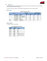
Modes
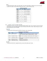
The following table shows the values to write to the SR_DATA_OUT register to set the Resolver to Digital Converter to various modes. Each
mode has two commands, one for the D0 wiper, and one for the D1 wiper. They may be written in any order.
Table 28: Channel Modes
Data
D1
D0
Mode
0xC080
0xC180
0V
0V
10-bit Synchro/Resolver
0xC0FF
0xC180
0V
5V
12-bit Synchro/Resolver
0xC080
0xC1FF
5V
0V
14-bit Synchro/Resolver
0xC0FF
0xC1FF
5V
5V
16-bit Synchro/Resolver
0xC080
0xC100
-5V
0V
8-bit LVDT
0xC000
0xC180
0V
-5V
10-bit LVDT
0xC000
0xC1FF
5V
-5V
12-bit LVDT
0xC000
0xC100
-5V
-5V
14-bit LVDT
7.5.3
C
HANNEL X
V
ELOCITY
T
RIM
(0
X
01
AND
0
X
03)
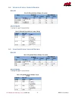
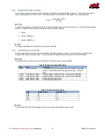
This shift register select line is connected to an Intersil ISL22424 digital potentiometer. Wiper 0 of the potentiometer is used to trim the velocity
gain of the control loop. Wiper 1 of the potentiometer is used to trim the velocity offset of the control loop. Velocity trimming is only required
when using the analog CHx_VELOCITY outputs.
Output Data
The Table below shows the value to write to the SR_DATA_OUT register to issue various commands.
Table 29: Velocity Trim Shift Register
Data
Name
Description
0x60C0
Set to Non-Volatile
All subsequent writes to the wiper position are only stored in non-volatile
memory. This should be done prior to adjusting the wiper, i.e. at board
open.
0xC0XX
Write Gain Trim Wiper
A value of 0x00 is minimum gain, 0x80 is nominal, and 0xFF is maximum
gain.
0xC1YY
Write Offset Trim Wiper
A value of 0x00 is most negative offset, 0x80 is nominal, and 0xFF is most
positive offset.
0x8000
Read Gain Trim Wiper
Reads the current wiper position.
0x8100
Read Offset Trim Wiper
Reads the current wiper position.
Input Data
The lower 8 bits of the SR_DATA_IN register contain the wiper position after a read command is issued

