RTD Embedded Technologies, Inc.
|
www.rtd.com
19
ERES35105
User’s Manual
5
Functional Description
Block Diagram
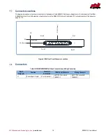
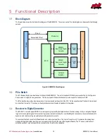
The Figure below shows the functional block diagram of the ERES35105. The various parts of the block diagram are discussed in the following
sections.
Figure 8: ERES35105 Block Diagram
PCIe Switch
The PCI Express Switch provides the bus interface to the ERES35105. The switch includes GPIO that are accessible from its Configuration
Space, which is configured as a generic bus. This is a low speed interface that does not provide support for interrupts or DMA.
The PCIe Switch also provides lane repopulation. One lane is used as the uplink to the CPU. On the opposite side of the board it is replaced
by a lane from the switch. This allows a virtually limitless number of boards to be added to the system.
Resolver to Digital Converter
The RD-19231 is a mixed signal CMOS IC containing analog input and digital output sections. Precision analog circuitry is merged with digital
logic to form a complete high-performance tracking resolver-to-digital converter. For user flexibility and convenience, the converter bandwidth,
dynamics, and velocity scaling are externally set with passive components.
The converter front-end consists of differential sine and cosine input amplifiers. The Control Transformer (CT) compares the analog input
signals with the digital output, resulting in an error signal proportional to the sine of the angular difference. The CT uses a combination of
amplifiers, switches, logic and capacitors in precision ratios to perform the calculation.
PCIe Switch
PC
Ie
Bu
s
J1
I/O C
on
ne
ct
or
PCIe x1
Link
Repopulated PCIe x1
EPLD
RD19231
Resolver to Digital
Converter
RD19231
Resolver to Digital
Converter
Front
End
Front
End
On-Board
Excitation

