


RFD900ux Data Sheet
www.rfdesign.com.au
7
Last update 12/09/2019
5
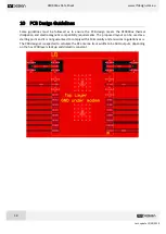
Performance characteristics
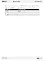
Figure 4-1 shows how the output power of the RFD900ux varies with supply voltage when the output
power is set to +30dBm.
Figure 4-1: Output power vs. input supply voltage
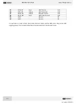
Figure 4-2 shows how the current through the RFD900ux varies with the transmit power level. The
current during transmission is shown by the ‘High Level’ plot and that during receive mode is shown
by the ‘Low Level’ plot.
Figure 4-1: Current consumption vs. TX power level
28
28.2
28.4
28.6
28.8
29
29.2
29.4
29.6
3.4
3.6
3.8
4
4.2
4.4
4.6
4.8
5
Po
w
er
Ou
tp
u
t
(d
Bm
)
Supply Voltage (Vcc)
0
100
200
300
400
500
600
700
800
900
0
5
10
15
20
25
30
35
Peak
Curr
en
t
(m
A)
Power Level (dBm)


