background image


RF-BM-2652P3 

www.szrfstar.com

                                                                                                                                                    V1.0 - Feb., 2021 

Shenzhen RF-star Technology Co., Ltd.                                                                                                                   

Page  6  of  20


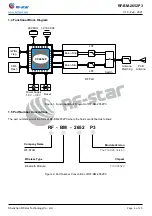
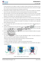
1.4 Functional Block Diagram 


Figure 1. Functional Block Diagram of RF-BM-2652P3 

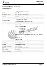
1.5 Part Number Conventions 

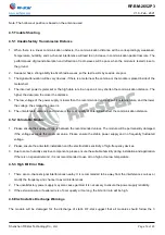
The part numbers are of the form of RF-BM-2652P3 where the fields are defined as follows: 


Figure 2. Part Number Conventions of RF-BM-2652P3 


CC2652P


GPIOs


Jtag


48.0 MHz


32.768 KHz


Reset


Balun Filter


Balun Filter


Power Supply


1.8 V ~ 3.8 V


Antenna 

Matching


Switch


PCB 

Antenna


8 Mb 

Flash


LPF


LPF


RF Part


RF


BM


2652


Company Name


RF-STAR


Wireless Type


Bluetooth Module


Chipset


TI CC2652P


-


-


P3


Module Version


The Third PA Version


Summary of Contents for SimpleLink RF-BM-2652P3

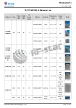
Page 1: ...1 0 Feb 2021 Shenzhen RF star Technology Co Ltd Page 1 of 20 RF BM 2652P3 SimpleLink Multiprotocol BLE5 1 ZigBee Wireless Module with Integrated Power Amplifier and Flash Version 1 0 Shenzhen RF star...

Page 2: ...CB 11 2 16 6 300 RF BM 4044B3 IPEX 11 2 15 2 500 RF BM 4044B4 CHIP 8 8 150 CC2640 R2FRGZ M3 128 28 5 RF BM 4077B1 PCB 17 23 5 500 CC2640 R2FRGZ Q1 RF BM 4077B2 PCB 17 23 5 500 CC2642R M4F 352 80 5 RF...

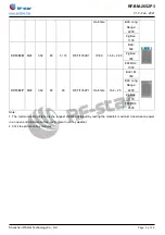
Page 3: ...IPEX 16 8 26 5 BLE 500 ZigBee 300 868 MHz 1000 CC1352P M4F 352 80 20 RF TI1352P1 Half hole 16 4 25 BLE 1M 350 BLE Long Range 2200 ZigBee 1100 868 MHz 2500 Note 1 The communication distance is the long...

Page 4: ...IEEE 802 15 4 PHY and MAC Excellent receiver sensitivity 100 dBm for 802 15 4 2 4 GHz 105 dBm for Bluetooth 125 kbps LE coded PHY Output power up to 20 dBm with temperature compensation Suitable for s...

Page 5: ...Sensor controller low power mode 2 MHz running infinite loop 30 1 A Sensor controller active mode 24 MHz running infinite loop 808 A Standby 0 94 A RTC on 80 KB RAM and CPU retention Shutdown 150 nA w...

Page 6: ...numbers are of the form of RF BM 2652P3 where the fields are defined as follows Figure 2 Part Number Conventions of RF BM 2652P3 CC2652P GPIOs Jtag 48 0 MHz 32 768 KHz Reset Balun Filter Balun Filter...

Page 7: ...2 1 Module Parameters 9 2 2 Module Pin Diagram 10 2 3 Pin Functions 10 3 Specifications 12 3 1 Recommended Operating Conditions 12 3 2 Handling Ratings 12 4 Application Implementation and Layout 13 4...

Page 8: ...6 Figure 3 Pin Diagram of RF BM 2652P3 10 Figure 4 Recommendation of Antenna Layout 15 Figure 5 Recommended Reflow for Lead Free Solder 18 Figure 6 Optional Packaging Mode 18 Table of Tables Table 1...

Page 9: ...Coded PHY GPIO 23 Power Consumption RX current 6 9 mA TX current 7 3 mA 0 dBm 9 6 mA 5 dBm 22 mA 10 dBm 85 mA dBm MCU 48 MHz CoreMark 3 4 mA 71 A MHz Sensor Controller 30 1 A Low Power Mode 2 MHz runn...

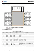
Page 10: ...SET RESET_N Reset active low No internal pullup resistor 2 ADC DIO16 Digital GPIO 3 GPIO04 DIO17 Digital GPIO 4 GPIO00 DIO24 Digital or Analog GPIO analog capability 5 SWO DIO25 Digital or Analog GPIO...

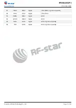
Page 11: ...chnology Co Ltd Page 11 of 20 11 TMSC TMSC Digital JTAG TMSC high drive capability 12 TCKC TCKC Digital JTAG TCKC 13 PWM2 DIO21 Digital GPIO 14 GPIO3 DIO20 Digital GPIO 15 RXD DIO5 Digital GPIO high d...

Page 12: ...fect the reliability of the module more or less Table 3 Recommended Operating Conditions of RF BM 2652P3 Items Condition Min Typ Max Unit Operating Supply Voltage 1 8 3 3 3 8 V Operating Temperature 4...

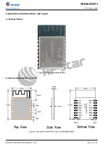
Page 13: ...0 Feb 2021 Shenzhen RF star Technology Co Ltd Page 13 of 20 4 Application Implementation and Layout 4 1 Module Photos Figure 3 Photos of RF BM 2652P3 4 2 Recommended PCB Footprint Figure 4 Recommende...

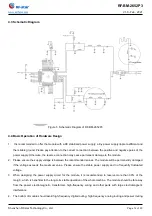
Page 14: ...mage to the module 2 Please ensure the supply voltage is between the recommended values The module will be permanently damaged if the voltage exceeds the maximum value Please ensure the stable power s...

Page 15: ...nded to stay away from the module according to the strength of the interference If circumstances permit appropriate isolation and shielding can be done 8 It is recommended to stay away from the device...

Page 16: ...voltage the smaller the power is 6 The unmatchable antennas and module or the poor quality of antenna will affect the communication distance 4 5 2 Vulnerable Module 1 Please ensure the supply voltage...

Page 17: ...soldering times 2 times based on the following reflow soldering profile 4 Temperature profile Reflow soldering shall be done according to the following temperature profile 5 Peak temperature 245 Tabl...

Page 18: ...www szrfstar com V1 0 Feb 2021 Shenzhen RF star Technology Co Ltd Page 18 of 20 Figure 5 Recommended Reflow for Lead Free Solder 4 8 Optional Packaging Figure 6 Optional Packaging Mode Note Default tr...

Page 19: ...ry Date Version No Description 2021 02 02 V1 0 The initial version is released Note 1 The document will be optimized and updated from time to time Before using this document please make sure it is the...
Page 20: ...OGY CO LTD Shenzhen HQ Add Room 601 Block C Skyworth Building High tech Park Nanshan District Shenzhen Guangdong China Tel 86 755 3695 3756 Chengdu Branch Add No B3 03 Building No 1 Incubation Park Hi...

Reviews: