background image

Renesas RA Family 

RA2 Quick Design Guide 

R01AN6060EU0100  Rev.1.00 


Page 40 of 44 

Sep.14.21 


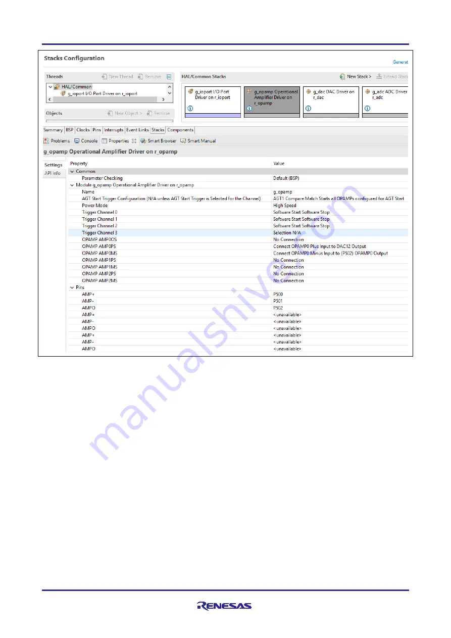
Figure 31.   Example of Setting A RA2A1’s OPAMP Using FSP Configurator 

After an OPAMP is set up by FSP Configurator, you can use OPAMP driver’s APIs such as 
R_OPAMP_Open and R_OPAMP_Start to initialize and start OPAMP operation. Refer to the  “Operational 
Amplifier (OPAMP)” chapter in RA2A1 Hardware User’s Manual and FSP User’s Manual for more details. 

16.  General Layout Practices 

16.1  Digital Domain vs. Analog Domain 

Renesas RA2 Microcontroller devices have three primary types of pin functions: Power, Digital, and Analog.  

Generally, power pins are dedicated for voltage and reference input and do not have multiple functions. 
Power pins are typically dedicated to specific portions, or domains, within the MCU. For example, the main 
supply voltage for the MCU will provide power to the digital core, many of the digital peripheral functions and 
many of the digital I/O pins. The digital domain can be defined as the digital circuitry, digital I/O pins, and the 
related power pins. Power pins which are designated for analog functions (such as AVCC0 and the 
associated AVSS0) supply specific analog circuitry within the MCU, which is separate from the digital domain 
circuitry. The analog domain can be defined as the analog circuitry, analog I/O pins, and the related power 
pins. 

Digital signals are typically repetitive, switched patterns that are associated with periodic clocks. The 
transitions on digital signals tend to be relatively sharp edges, with stable levels of high or low between the 
transitions. Each signal must be stable at an acceptable voltage level, referred to as a logic state, within a 
specified timeframe. The state of the signal is typically sampled at predetermined clock intervals, using the 
edge transition of a clock to evaluate the associated data signals. Small variations in the voltage level of 
digital signals are typically acceptable, as long as the level remains within a specified range. However, large 

Summary of Contents for RA2 Series

Page 1: ...s 4 1 1 References 5 2 Emulator Support 6 2 1 SWD Interface 7 2 2 Serial Programming Interface using SCI 8 2 3 Combination Debug Interface 9 3 MCU Operating Modes 9 4 Option Setting Memory 10 4 1 Option Setting Memory Registers 11 5 Clock Circuits 12 5 1 Reset Conditions 13 5 2 Clock Frequency Requirements 13 5 2 1 Requirements for USB Communications 14 5 2 2 Requirements for Programming and Erasi...

Page 2: ...ess 24 8 Register Write Protection 24 9 I O Port Configuration 25 9 1 Multifunction Pin Selection Design Strategies 25 9 2 Setting Up and Using a Port as GPIO 25 9 2 1 Internal Pull Ups 27 9 2 2 Open Drain Output 27 9 2 3 Drive Capacity 27 9 3 Setting Up and Using Port Peripheral Functions 27 9 4 Setting Up and Using IRQ Pins 28 9 5 Unused Pins 30 9 6 Nonexistent Pins 31 9 7 Electrical Characteris...

Page 3: ...ide R01AN6060EU0100 Rev 1 00 Page 3 of 44 Sep 14 21 16 General Layout Practices 40 16 1 Digital Domain vs Analog Domain 40 16 2 High Speed Signal Design Considerations 41 16 3 Signal Group Selections 41 17 References 42 Revision History 44 ...

Page 4: ... ground pin Connect this pin to VSS VCC_DCDC 2 Switching regulator power supply In DCDC mode connect this pin to VCC Connect this pin to VSS through a 0 1 µF capacitor placed close to the VCC_DCDC pin In LDO mode leave this pin open VSS_DCDC 2 Switching regulator ground pin In DCDC mode connect this pin to VSS In LDO mode leave this pin open VLO Switching regulator pin In DCDC mode connect this pi...

Page 5: ... with the SBIAS output As an input this pin has a voltage range of 0 8 V to 2 4 V set in 0 2 V increments Connect this pin to AVSS1 through a 0 22 µF capacitor Notes 1 For RA2A1 this applies to the 16 bit ADC 2 Present on RA2A1 only 3 Not present on RA2E2 4 For RA2E2 connect VREFH0 to VCC and VREFL0 to VSS if the 12 bit ADC is not used 1 1 References Further information regarding the power supply ...

Page 6: ... D A Converter 12 bit D A Converter If you plan to use the on chip A D or D A converters these chapters give details on how to provide filtered power supplies for these peripherals Clock Generation Circuit Provides detailed descriptions on how to configure and use the available clocks including PCB design recommendations 2 Emulator Support RA2 MCU devices have an emulator interface that supports b...

Page 7: ... Family RA2 Quick Design Guide R01AN6060EU0100 Rev 1 00 Page 7 of 44 Sep 14 21 2 1 SWD Interface Figure 1 SWD Interface Connections Note 1 The output of the reset circuit of the user system must be open collector ...

Page 8: ...Guide R01AN6060EU0100 Rev 1 00 Page 8 of 44 Sep 14 21 2 2 Serial Programming Interface using SCI Figure 2 Serial Programming Interface using SCI Connections Note 1 The output of the reset circuit of the user system must be open collector ...

Page 9: ...et circuit of the user system must be open collector 3 MCU Operating Modes The RA2 MCU series can enter one of two modes after reset Single chip mode or SCI USB boot mode The boot mode is selected by the MD pin Table 4 Operating Modes Available at Reset Operating Mode MD On Chip Flash Memory Single chip mode 1 Enable SCI USB boot mode 0 Enable Figure 4 shows operating mode transitions as determine...

Page 10: ...e code flash memory map Although the registers are located in a portion of the flash memory that was reserved on the RA MCUs it is possible that some customers may store data in these locations inadvertently The user must check to ensure that no unwanted data is written to these locations or else unexpected behavior of the chip may result Additionally when using binary files for programming the us...

Page 11: ...Make sure that they are configured properly before startup OFS0 register Independent Watchdog Timer IWDT auto start IWDT timeout frequency windowing interrupt type and low power mode behavior Watchdog Timer WDT auto start WDT timeout frequency windowing and interrupt type OFS1 register LVD0 enable after reset HOCO startup after reset Renesas FSP Configurator supports setting of option memory in BS...

Page 12: ... directed to the main system clock ICLK flash clock CPU clock and peripheral module clocks For some devices the clock distribution also includes additional clocks for ADC and USB peripherals Note that RA2E2 devices do not have external crystal or clock input pins Refer to the Hardware User s Manual Clock Generation Circuit chapter for the block diagram of the clock generation circuit Each clock ha...

Page 13: ...endently from MOSC and can be sourced from MOSC SOSC HOCO MOCO or LOCO 4 Not present on RA2E2 Some devices such as RA2E2 do not include the option for an external crystal or clock In this case the oscillator sources for the main clock are limited to the on chip oscillators 5 1 Reset Conditions After reset RA2 MCUs begin running with the middle speed on chip oscillator MOCO as the main clock source...

Page 14: ...by setting the appropriate register s The registers for controlling each clock source are shown in the table below Table 7 Clock Source Configuration Registers Oscillator Register Description Main clock 1 MOSCCR Starts stops main clock oscillator Sub clock 1 SOSCCR Starts stops sub clock oscillator High speed on chip HOCO HOCOCR Starts stops HOCO Middle speed on chip MOCO MOCOCR Starts stops MOCO ...

Page 15: ...re 9 Clock Settings Using Renesas FSP Configurator 5 6 HOCO Accuracy The internal high speed on chip oscillator HOCO runs at 24 MHz 32 MHz 48 MHz or 64 MHz for RA2 devices with a typical accuracy of 2 or better HOCO accuracy specifications are characterized for various ambient operating temperature Ta ranges See the Electrical Characteristics of the Hardware User s Manual for the clock accuracy sp...

Page 16: ...d Design Refer to the Usage Notes section of the Clock Generation Circuit CGC chapter in the Hardware User s Manual for more information on using the CGC and for board design recommendations In general place the crystal resonator and its load capacitors as close to the MCU clock pins XTAL EXTAL XCIN XCOUT as possible Avoid routing any other signals between the crystal resonator and the MCU Minimiz...

Page 17: ...e crystal resonator components 5 10 External Clock Input A digital clock input may be used as the main clock source for most RA2 devices Figure 12 shows an example of connecting an external clock input To operate the oscillator with an external clock signal set the MOMCR MOSEL bit to 1 The XTAL pin becomes high impedance Figure 12 Equivalent circuit for external clock Notes The frequency of the ex...

Page 18: ...ate a power on reset POR 1 If the RES pin is in a high level state when power is supplied 2 If the RES pin is in a high level state when VCC is below VPOR After VCC has exceeded the power on reset voltage VPOR and the power on reset time tPOR has elapsed the chip is released from the power on reset state The power on reset time is a period that allows for stabilization of the external power supply...

Page 19: ...andling Refer to MCU User s Manual for the specific timing For details on the SYSRESETREQ bit see the ARM Cortex M23 Technical Reference Manuals 6 7 Other Resets Most peripheral functions within the MCU can generate a reset under specific fault conditions No hardware configuration is required to enable these resets Refer to the relevant chapters in the Hardware User s Manual for details of the con...

Page 20: ...s are used to access each increasing performance and allowing same cycle access of program and data Contained within the memory map are regions for on chip RAM peripheral I O registers program code flash and data flash Figure 13 RA2A1 Memory Map 7 1 SRAM The RA2 MCUs provide on chip SRAM modules with either parity bit checking or ECC Error Correction Code The following table lists the SRAM specifi...

Page 21: ...d data flash which vary in size and programmable cycle capacity by device The Flash Control Unit FCU controls programming and erasure of the flash memory The Flash Application Command Interface FACI controls the FCU in accordance with the specified FACI commands The code flash is designed to store user application code and constant data The data flash is designed to store information that may be u...

Page 22: ...ile the code flash memory is being erased or programmed The only exception to this rule is that the data flash cannot be accessed during code flash programming or erasing 7 3 2 ID Code Protection RA2 MCUs have a 128 bit memory in option setting memory area that is used as an ID code If this ID code is left blank 0xFF s then no protection is enabled and access to the MCU is allowed through boot mod...

Page 23: ...ing access to the MCU 7 3 3 Memory Protection Unit RA2 MCUs have a Memory Protection Unit MPU The MPU has the ability to protect various MCU regions from illegal access The choices include allowing both reading and writing prohibiting writing and prohibiting writing and reading Select one of these options by setting the corresponding constant value at the specific memory address See Memory Protect...

Page 24: ...n Endianness Memory space must be little endian to execute code on the Cortex M core 8 Register Write Protection The register write protection function protects important registers from being overwritten because of software errors The registers to be protected are set with the Protect Register PRCR Table 9 lists the association between the PRCR bits and the registers to be protected b15 b14 b13 b1...

Page 25: ...ter a reset There may be a small period where some pins may be in an undesirable state This will be true regardless of what configuration approach is used The user should consider the impact this may have for each application including how this may affect other system features The IO Port Configuration may be set using either direct write to registers or using the FSP Pin Configurator 9 1 Multifun...

Page 26: ...pecify whether individual pins function as GPIO or as peripheral pins Out of reset all PMR registers are set to 0 which sets all pins to work as GPIO If a PMR register is set to 1 then that corresponding pin will be used for peripheral functions The peripheral function is defined by that pin s MPC setting When setting a pin as an output it is recommended that the desired output value of the port b...

Page 27: ...controlled by the Drive Capacity Control Register DSCR bits in each Port mn Pin Function Select PmnPFS register Out of reset all DSCR registers are cleared to 0 Therefore all pins are set to low drive output Setting a value other than 00 will change the drive capacity of the output for the selected pin The maximum total output of all pins is dependent on the specific MCU group and device package P...

Page 28: ...e user should not do this but the MCU will allow it If this occurs the function on the pins will be undefined Figure 20 shows an example of enabling SPI0 pins using FSP Pin configuration Figure 20 Enabling SPI0 pins using Pin Configurator in Renesas FSP 9 4 Setting Up and Using IRQ Pins Certain port pins can be used as hardware interrupt lines IRQ See the Peripheral Select Settings for each Produc...

Page 29: ...e enabled for each IRQ pin independently This is done by setting the IRQ Pin Digital Filter Enable FLTEN bit in the IRQCRi register for each IRQ The clock rate for digital filtering is configurable for each IRQ pin independently This is done by setting the IRQ Pin Digital Filter Setting FCLKSEL 1 0 bits in the IRQCRi register for each IRQ Figure 21 and Figure 22 show examples of enabling and confi...

Page 30: ...ng a pin directly to VCC or VSS since an accidental write to the port s direction register that sets the pin to an output could create a shorted output 2 A second method is to set the pin to an output The pin level may be set high or low However setting the pin as an output and making the output low connects the pin internally to the ground plane This may help with overall system noise concerns A ...

Page 31: ...y different input requirements See the Hardware User s Manual section Electrical Characteristics for more information 10 Module Stop Function To maximize power efficiency the RA2 series of MCUs allow on chip peripherals to be stopped individually by writing to the Module Stop Control Registers MSTPCRi i A B C D Once a module stops access to the module registers is not possible After a reset most o...

Page 32: ...4 Sep 14 21 Figure 23 RA2A1 ICU Specifications Figure 24 RA2A1 ICU I O Pins Figure 25 is an example of using a Renesas FSP configurator to enable and configure an interrupt using Renesas FSP The ICU and interrupts are configured as part of the HAL driver configuration through FSP ...

Page 33: ...l functions for reducing power consumption These include setting clock dividers stopping modules selecting power control mode in Normal mode and transitions to low power modes Refer to the chapter Low Power Modes in the Hardware User s Manual for more details RA2 MCUs support three different types of LPM These are Sleep mode Software Standby mode Snooze mode The following table is an overview of t...

Page 34: ...e are supported Table 12 lists the conditions to transition to low power modes the states of the CPU and the peripheral modules and the method for cancelling each mode Table 12 Low Power Consumption Modes State of operation 1 Sleep Mode All Module Clock Stop Mode Software Standby Mode Transition condition WFI instruction while SBYCR SSBY 0 WFI instruction while SBYCR SSBY 1 and DPSBYCR DPSBY 0 Sno...

Page 35: ...t the requirements of the desired mode Otherwise the settings in the OPCCR register will not have any effect in lowering power consumption In order to achieve the lowest power numbers use the maximum possible dividers in the clock generation circuits Low power modes are canceled by various interrupt sources such as RES pin reset power on reset voltage monitor reset and peripheral interrupts Refer ...

Page 36: ...rr Transition to configured LPM mode Deep Software Standby Mode err R_LPM_LowPowerModeEnter g_lpm_sw_standby_ctrl Handle error if FSP_SUCCESS err return err 13 Buses The buses in RA2 MCUs consist of a main bus and a slave interface Figure 27 lists the main bus and the slave interface Figure 28 shows the bus configuration Note Memory space must be little endian in order to execute Cortex code Figur...

Page 37: ...returned to the requesting master IP The bus error information that occurred in each master is stored in the BUSnERRADD and BUSnERRSTAT registers These registers must be cleared by reset only For more information see section Bus Error Address Register BUSnERRADD and Bus Error Status Register BUSnERRSTAT in the Hardware User s Manual Note The DTC do not receive bus errors so their operation is not ...

Page 38: ...Renesas RA Family RA2 Quick Design Guide R01AN6060EU0100 Rev 1 00 Page 38 of 44 Sep 14 21 Figure 29 SDADC24 Specifications 1 of 2 ...

Page 39: ... consumption Operation can be started by a trigger from the Asynchronous General Purpose Timer AGT Operation can be stopped by a 16 bit A D conversion end trigger All units have switches that can select input signals Additionally OPAMP0 has a switch that can select the output pin The output of the OPAMP can be output from the AMP0O to AMP2O pins without passing through the switch The I O signals o...

Page 40: ...eripheral functions and many of the digital I O pins The digital domain can be defined as the digital circuitry digital I O pins and the related power pins Power pins which are designated for analog functions such as AVCC0 and the associated AVSS0 supply specific analog circuitry within the MCU which is separate from the digital domain circuitry The analog domain can be defined as the analog circu...

Page 41: ...ions it is highly recommended to evaluate the specific design using simulation tools to understand the effect that circuit design has on the performance For example this may include applications such as precision sensor designs or very high speed digital bus interfaces Refer to the Electrical Characteristics chapter in the Hardware User s Manual for the specific requirements for each peripheral fu...

Page 42: ...dware User s Manual 17 References The following documents were used in creating this Quick Design Guide Visit Renesas website for the latest version of each of these documents Reference Document Number Description 1 R01UH0888 Renesas RA2A1 Group User s Manual Hardware 2 R01UH0852 Renesas RA2E1 Group User s Manual Hardware 3 R01UH0853 Renesas RA2L1 Group User s Manual Hardware 4 R01UH0919 Renesas R...

Page 43: ...t the following vanity URLs to learn about key elements of the RA family download components and related documentation and get support RA Product Information www renesas com ra RA Product Support Forum www renesas com ra forum RA Flexible Software Package www renesas com FSP Renesas Support www renesas com support ...

Page 44: ...Renesas RA Family RA2 Quick Design Guide R01AN6060EU0100 Rev 1 00 Page 44 of 44 Sep 14 21 Revision History Rev Date Description Page Summary 1 00 Sep 14 21 Initial release ...

Page 45: ...ons failure or accident arising out of the use of Renesas Electronics products outside of such specified ranges 7 Although Renesas Electronics endeavors to improve the quality and reliability of Renesas Electronics products semiconductor products have specific characteristics such as the occurrence of failure at a certain rate and malfunctions under certain use conditions Unless designated as a hi...

Reviews: