background image

M3062PT3-RPD-E User’s Manual 

2. Setup 

REJ10J0040-0600 Rev.6.00 July 01, 2006 


Page 37 of 104 


2.8.7 Connecting to a 100-pin 0.5mm Pitch Foot Pattern (Part 2) 

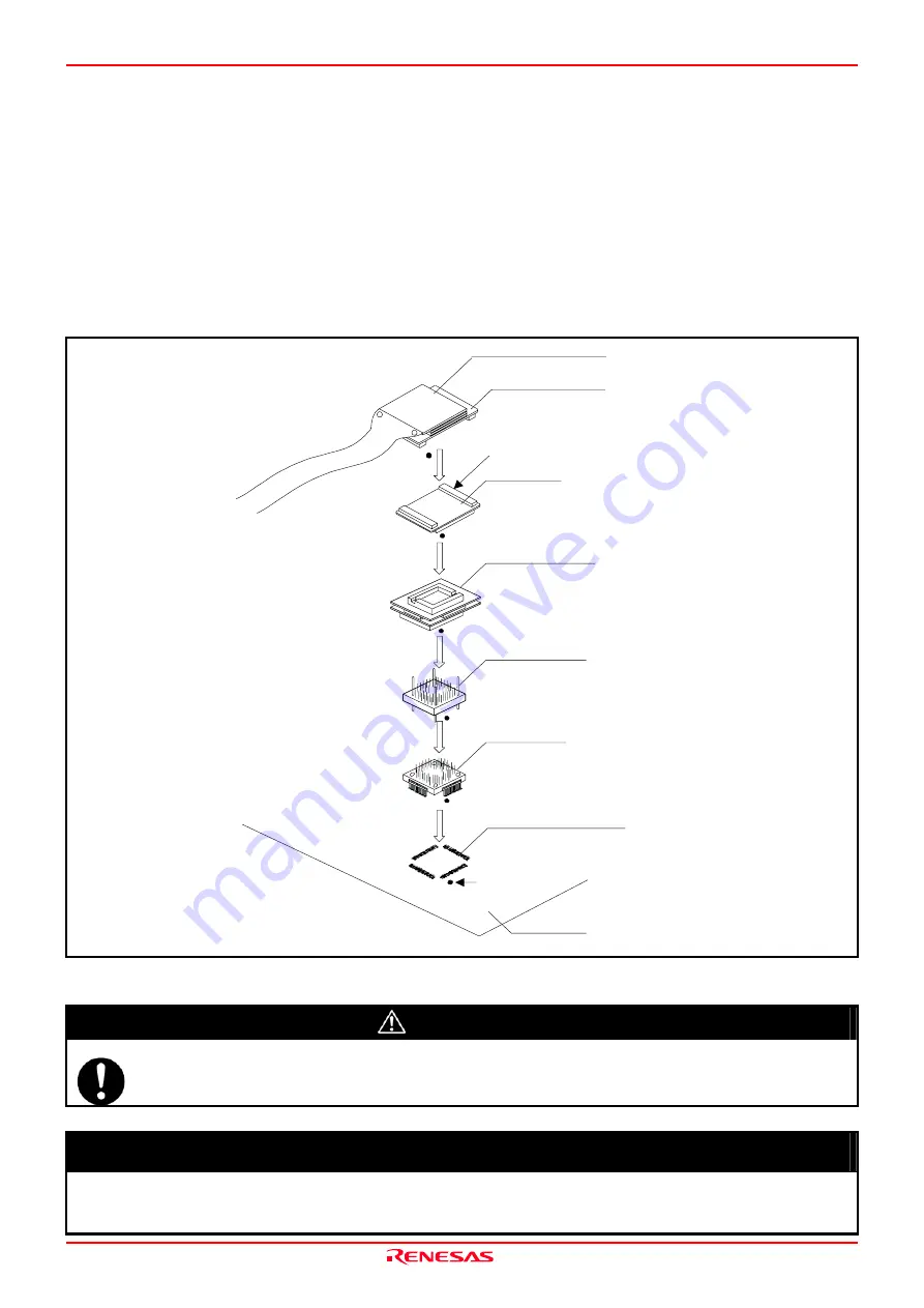
Figure 2.15 shows how to connect a 100-pin 0.5mm pitch foot pattern on the user system to the M3T-100LCC-QSD (not 
included), and here following is its procedure. For details on the M3T-100LCC-QSD (not included), refer to its user's manual. 
 
(1)


Attach the TQPACK100SD to the user system. 

(2)


Attach the TQSOCKET100SDG to the TQPACK100SD. 

(3)


Attach the M3T-100LCC-QSD to the TQSOCKET100SDG. 

(4) Attach the CN2 side of the M30800T-PTC to the CN2 side of the package converter board connected to the emulation pod 

probe. 

(5)  Attach the M30800T-PTC to the M3T-100LCC-QSD. 


Figure 2.15 Connecting to a 100-pin 0.5mm pitch foot pattern (2/2) 


CAUTION


Note on Connecting the User System: 


z


Take care not to attach the converter board in a wrong direction. It may cause a fatal damage to the emulation 
pod. 


IMPORTANT


Notes on Connectors of the Converter board: 


z


The connectors of the M30800T-PTC are guaranteed for only 50 insertion/removal iterations. 

z


The connectors of the M3T-100LCC-QSD are guaranteed for only 20 insertion/removal iterations. 

M3T-100LCC-QSD

(not included)

CN2 side

(4)

(5)

M30800T-PTC

(3)

(2)

TQSOCKET100SDG

TQPACK100SD

Package converter board

Tip of emulation pod probe

(1)

100-pin 0.5mm pitch

(PLQP0100KB-A) foot pattern

No. 1 pin

User system

Summary of Contents for Emulation Pod M3062PT3-RPD-E

Page 1: ...REJ10J0040 0600 T M3062PT3 RPD E Rev 6 00 Jul 01 2006 User s Manual Emulation Pod for M16C 62P and M16C 30P Groups...

Page 2: ...l inaccuracies or typographical errors Renesas Technology Corp assumes no responsibility for any damage liability or other loss rising from these inaccuracies or errors Please also pay attention to in...

Page 3: ...are shown in 1 1 Package components page 13 If there is any question or doubt about this product contact your local distributor The related manuals for using this product are listed below You can dow...

Page 4: ...for use in your program development and evaluation stages In mass producing your program you have finished developing be sure to make a judgment on your own risk that it can be put to practical use b...

Page 5: ...nstantly making efforts to improve the design and performance of this emulator Therefore the specification or design of this emulator or its user s manual may be changed without prior notice About the...

Page 6: ...es an imminently dangerous situation that will cause death or heavy wound unless it is avoided However there are no instances of such danger for the product presented in this user s manual WARNING WAR...

Page 7: ...that a reliable ground connection is maintained z If you smell a strange odor hear an unusual sound or see smoke coming from this product then disconnect power immediately by unplugging the AC power c...

Page 8: ...interface cable or the flexible cable for connecting the user system And excessive flexing or force may break conductors z Do not pull the flexible cable FLX120 RPD for connecting to the emulator mai...

Page 9: ...3 LED Display When the Emulator Starts Up Normally 26 2 6 Downloading Firmware 27 2 6 1 When It is Necessary to Download Firmware 27 2 6 2 Downloading Firmware in Maintenance Mode 27 2 7 Self check 28...

Page 10: ...oprocessor Mode Vcc1 Vcc2 3V 78 4 3 Differences between the Actual MCU and Emulator 83 4 4 Connection Diagram 86 4 5 External Dimensions 88 4 5 1 External Dimensions of the Emulation Pod 88 4 5 2 Exte...

Page 11: ...it by email you can use a text format for user registration created when installing the software in the following folder Your registered information is used for only after sale services and not for a...

Page 12: ...emulator debugger This means a software tool starting up from the High performance Embedded Workshop to control the emulator and this product and enables debugging Firmware Program that analyzes conte...

Page 13: ...nics Co Ltd 1 OSC 3 16MHz oscillator circuit board for main clock preinstalled 1 OSC 2 oscillator circuit board bare board 1 Network resistors for pulling up ports P0 P5 51k x 8 6 H W Tool Customer Re...

Page 14: ...ing the PC4700L and PC4701L M16C PC4701 Emulator Debugger Emulator debugger M3T PD30 Included with the PC4701 80 pin 0 65mm pitch QFP PRQP0080JA A Previous code 80P6S A M3062PT 80FPB M3T F160 100NRB M...

Page 15: ...ting the emulation pod and the user system 4 Converter board M30800T PTC included This is a converter board for connecting to 100 pin 0 65mm pitch LCC socket IC61 1004 051 on the user system For detai...

Page 16: ...s of the system status LEDs Name Status Meaning ON Emulator system power supply is turned ON POWER OFF Emulator system power supply is turned OFF ON Emulator system is operating normally Flashing Spec...

Page 17: ...er program has been halted ON CPU clock of target MCU is not oscillating HALT OFF CPU clock of target MCU is oscillating IMPORTANT Note on the Target Status POWER LED z If the MCU has two or more Vcc...

Page 18: ...lay C level debugging etc Real time trace function 32K cycle bus information recordable Bus external trigger time stamp 5 trace modes supported Break Before About After Full Can be recorded ON OFF by...

Page 19: ...g the User System page 30 128 pin 0 5mm pitch LQFP PLQP0128KB A Previous code 128P6Q A 1 M3T F160 128NRD not included 1 5 Operating Environment Be sure to use this emulator with the operating environm...

Page 20: ...to the using interface Connect the emulation pod to the emulator Connect the emulation pod M3062PT3 RPD E to the PC4701 using the FLX120 RPD Connect the power supply for the emulator Connect a power...

Page 21: ...wnloading the M16C PC4701 Emulator Debugger as occasion demands Download the latest M16C PC4701 Emulator Debugger from the URL below free of charge http download renesas com eng mpumcu upgrades in_cir...

Page 22: ...oard PCA4202G02 discontinued product is required on the host machine side Serial RS232C The RS232C interface cable 25 pin female 25 pin female conversion cable and 25 pin female 9 pin female conversio...

Page 23: ...0 RPD Figure 2 2 Connecting the FLX120 RPD to the PC4701 CAUTION Note on Connecting the PC4701 and FLX120 RPD z Always shut OFF power before connecting the cable Otherwise the internal circuits may be...

Page 24: ...e FLX120 RPD to the emulation pod CAUTION Note on Connecting the FLX120 RPD and emulation pod z Always shut OFF power before connecting the emulation pod and the FLX120 RPD Otherwise the internal circ...

Page 25: ...ecause of leakage current the internal circuits may be damaged When turning ON the power again after shutting OFF the power wait for about 10 seconds IMPORTANT Notes on Power Supply z The emulator s p...

Page 26: ...off when both main and sub clocks are not oscillating If either clock is oscillating the LED is turned on z If the LED is not turned on check the following 1 After powering on the PC4701 before start...

Page 27: ...face The firmware may not be downloaded in maintenance mode correctly with the USB interface 2 Within 2 seconds of activating power to the emulator press the RESET switch on the PC4701 upper panel to...

Page 28: ...s blinking and then press the system reset switch again 5 The self check will start If the normal result is displayed in about 30 seconds the self check has terminated normally Figure 2 6 LED display...

Page 29: ...r the switch settings of this product are the factory settings IMPORTANT Notes on Self check z Perform the self check while not connecting the user system z If the self check does not result normally...

Page 30: ...n QFP M3T DUMMY100S 100 pin QFP M3T F160 100NSD 100 pin LQFP M3T 100LCC QSD 100 pin LQFP M3T F160 128NRD 128 pin LQFP 100 pin 80 pin 0 65mm pitch M 3062PT 80FPB 80 pin QFP M3T F160 100NRB 100 pin QFP...

Page 31: ...of the package converter board connected to the emulation pod probe 4 Attach the M3062PT 80FPB to the YQPACK080SB CN2 side 3 1 80 pin 0 65mm pitch PRQP0080JA A foot pattern No 1 pin User system M3062P...

Page 32: ...in LCC socket CN 2 side 1 No 1 pin 2 M 30800T PTC User system Package converter board Tip of emulation pod probe Figure 2 10 Connecting to a 100 pin LCC socket CAUTION Note on Connecting the User Syst...

Page 33: ...e of the package converter board connected to the emulation pod probe 4 Attach the M3T F160 100NRB to the YQPACK100RB Figure 2 11 Connecting to a 100 pin 0 65mm pitch foot pattern 1 3 CAUTION Note on...

Page 34: ...converter board connected to the emulation pod probe 4 Attach the M30800T PTC to the M3T 100LCC DMS Figure 2 12 Connecting to a 100 pin 0 65mm pitch foot pattern 2 3 CAUTION Note on Connecting the Use...

Page 35: ...nnected to the emulation pod probe 4 Attach the M30800T PTC to the M3T 100LCC DMS Figure 2 13 Connecting to a 100 pin 0 65mm pitch foot pattern 3 3 CAUTION Note on Connecting the User System z Take ca...

Page 36: ...side of the package converter board connected to the emulation pod probe 4 Attach the M3T F160 100NSD to the YQPACK100SD CN 2 side 3 1 100 pin 0 5 mm pitch PLQP 0100KB A foot pattern No 1 pin User sys...

Page 37: ...of the package converter board connected to the emulation pod probe 5 Attach the M30800T PTC to the M3T 100LCC QSD Figure 2 15 Connecting to a 100 pin 0 5mm pitch foot pattern 2 2 CAUTION Note on Conn...

Page 38: ...ide of the package converter board connected to the emulation pod probe 4 Attach the M3T F160 128NRD to the YQPACK128RD CN2 side 3 1 128 pin 0 5mm pitch PLQP0128KB A foot pattern No 1 pin User system...

Page 39: ...ove the four screws of both sides of the M3062PT3 RPD E and lift off the upper cover see Figure 2 17 2 Attaching the upper cover To close the upper cover attach the upper cover and secure the four scr...

Page 40: ...rcuit board 2 Position of switches 3 Position of socket for mounting network resistor for pullup 4 Position of bypass capacitor for A D converter Figure 2 18 Positions of each part MCU dependent board...

Page 41: ...UT External User system Internal Internal oscillator circuit of emulation pod 32 768kHz Sub XCIN XCOUT External User system Yes IMPORTANT Notes on Changing the Clock Supply z The clock supply can be s...

Page 42: ...1 Unscrew the screw securing the oscillator circuit board 2 Lift off the oscillator circuit board 3 Insert the connector of a new oscillator circuit board to the connector of the main board 4 Secure t...

Page 43: ...e located Figure 2 21 shows the circuitry of the OSC 2 oscillator circuit board bare board Use the number of oscillator circuits recommended by the oscillator manufacturer Figure 2 20 External view of...

Page 44: ...of the evaluation MCU into pin XIN And pin XOUT should be open Choose External in the emulator debugger to use this clock Figure 2 22 External oscillator circuit Make note that in the oscillator circu...

Page 45: ...E of the MCU with a resistance of 33k BYTE H OPEN L SW1 Use this setting when the user system is connected Does not pull up down pin BYTE of the MCU Inputs the level of the user system to pin BYTE of...

Page 46: ...ngs Connects pin P86 Xcout of the MCU to the user system to use it as port P86 or Xcout P86 Xcout SW4 P86 Xcout SW4 P86 XC OP Does not connect pin P86 Xcout of the MCU to the user system P87 Xcin P87...

Page 47: ...M3062PT3 RPD E 3 Signal Switch Setting Description A18_SEL 1M JP1 4M factory settings Always use this setting A18_SEL JP1 A18_SEL 1M JP1 4M Do not use this setting VDDIO VCC1 VCC2 JP2 VCC1 VCC2 facto...

Page 48: ...mounting location refer to Figure 2 24 below And for the positions of each part refer to Figure 2 18 Figure 2 24 Position for mounting network resistors for pullup CAUTION Note on Installing and Remov...

Page 49: ...ss capacitors as occasion demands Figure 2 18 shows where they are installed and Figure 2 25 shows their connection Figure 2 25 Foot patterns of bypass capacitors for A D converter IMPORTANT Note on t...

Page 50: ...ugger is installed The emulator debugger has been installed in the following directory by default When using the M16C PC4701 emulator debugger on the High performance Embedded Workshop C Program Files...

Page 51: ...expansion or microprocessor mode the areas listed below cannot be used as a work area specify a work area other than the areas listed below And the top address of the work area should be an even numbe...

Page 52: ...list Select SessionM16C_PC4701_Emulator 3 3 1 Init Dialog Box After specifying the session an Init dialog box to connect the target is displayed The Init dialog box is used to set the items that need...

Page 53: ...For I O address setting of PCA4202G02 refer to the PCA4202G02 Instruction Manual Specifying the communication interface Serial For connection with serial communication click the radio button Serial o...

Page 54: ...the emulator you are going to connect 3 Executing the self check Executing the self check Enable this function when you want the emulator to be self checked at startup Be sure to select the check box...

Page 55: ...mpiler you are using and the format of the object file output by the compiler To make this setting use the dialog box that is brought up by selecting Debug and then Debug Settings from the menu Specif...

Page 56: ...ess of the work area is set to 2C00h by default In single chip mode set the work area address at 10000h 4 Memory space expansion tab Specifying the memory space expansion mode When the memory expansio...

Page 57: ...button brings up a file selection dialog box The script file you have selected is displayed in the Init File section of the dialog box shown here If you do not want to automatically execute a script c...

Page 58: ...ystem Check to see that the emulator debugger has been connected correctly to the emulator Checking connections of the emulator system When the emulator debugger is connected correctly to the emulator...

Page 59: ...rom xxx x30 of Download module Or you can select Download module from the Debug menu for the same effect 2 Showing the source program Editor Source window The editor source window is a window that alw...

Page 60: ...s the program after resetting the target MCU Step In Single steps the program executing each statement including those in functions Step Over Single steps the program executing each function call as o...

Page 61: ...break point setting line on the software break point setting column in the editor source window the break point can be set up and released In this case the red circle is displayed on the setting line...

Page 62: ...me command 1 Specifying the Come command Setup procedure for executing COME command 1 Click the line in the editor source window at which you want the program to execute 2 Click the Come button 2 Afte...

Page 63: ...ware break point setup dialog box 2 H W Break Points Setting Window H W Break Points Setting Window Select the Enable H W Break check box and this break function will be enabled allowing you to set ha...

Page 64: ...er REJ10J0040 0600 Rev 6 00 July 01 2006 Page 64 of 104 2 When FETCH is selected 1 Window for setting addresses Setting the address You can set eight conditions e g a specified address a specified add...

Page 65: ...You can set eight conditions e g a specified address a specified address range etc When you have finished setting the address set the data 2 Window for setting data Setting data Sets the address by Da...

Page 66: ...ts for bytewise accesses to the odd addresses STE B R0L A1A0 R0L E6h A1 0000h A0 20E3h High order data effective Setting a break event A1 Address 1 0020E3 Data 1 00E6 MASK 00FF Access WRITE 4 Setting...

Page 67: ...as the following four display modes Mixed mode also can be displayed Bus mode Bus information per cycle can be inspected The contents are displayed in order of execution paths Disassemble mode The exe...

Page 68: ...ive DMA Data access except for CPU INT Interrupt acknowledge cycle IB Instruction code read bytes by CPU DB Data access bytes by CPU IW Instruction code read words by CPU DW Data access words by CPU R...

Page 69: ...00 July 01 2006 Page 69 of 104 2 Suspending and resuming trace measurement 1 Suspending trace measurement Suspend Click this toolbar button to suspend the trace measurement in progress 2 Resuming trac...

Page 70: ...trace point condition was met is recorded Full 32K cycles of instruction execution after a trace began is recorded 2 Setting the trace write condition Setting the trace write condition You can specify...

Page 71: ...anges of memory contents while the user program is executed This is accomplished by using the real time RAM monitor function and the memory contents corresponding to the RAM monitor area are displayed...

Page 72: ...plicable MCU M16C 60 Series M16C 62P Group M16C 30 Series M16C 30P Group Evaluation MCU M30627MHPGP M30627FHPGP Applicable MCU mode Single chip mode Memory expansion mode NORMAL 4MB Microprocessor mod...

Page 73: ...BCLK standard 4 See left th RD AD Address output hold time RD standard 0 1 th WR AD Address output hold time WR standard 2 See left td BCLK CS Chip select output delay time 25 See left th BCLK CS Chip...

Page 74: ...Read timing Write timing BCLK ADi ALE DBi td BCLK CS th BCLK CS tcyc td BCLK AD th BCLK AD th RD CS td BCLK ALE th BCLK ALE th RD AD td BCLK RD th BCLK RD tac2 RD DB Hi Z tsu DB RD th RD DB BCLK ADi...

Page 75: ...BCLK RD RD signal output hold time 0 1 td BCLK WR WR signal output delay time 25 See left th BCLK WR WR signal output hold time 0 4 td BCLK DB Data output delay time BCLK standard 40 See left th BCLK...

Page 76: ...ming BCLK ADi ALE ADi DBi td BCLK CS th BCLK CS tcyc td BCLK AD th BCLK AD th RD CS td BCLK ALE th BCLK ALE th RD AD td BCLK RD th BCLK RD tac3 RD DB Hi Z tsu DB RD th RD DB BCLK ADi ALE ADi DBi td BC...

Page 77: ...setup time 40 80 th RD DB Data input hold time 0 See left th BCLK RDY RDY input hold time 0 See left th BCLK HOLD HOLD input hold time 0 See left td BCLK HLDA HLDA output delay time 40 See left Compar...

Page 78: ...WR standard 2 See left td BCLK CS Chip select output delay time 30 See left th BCLK CS Chip select output hold time BCLK standard 4 See left td BCLK ALE ALE signal output delay time 30 See left th BCL...

Page 79: ...Read timing Write timing BCLK ADi ALE DBi td BCLK CS th BCLK CS tcyc td BCLK AD th BCLK AD th RD CS td BCLK ALE th BCLK ALE th RD AD td BCLK RD th BCLK RD tac2 RD DB Hi Z tsu DB RD th RD DB BCLK ADi...

Page 80: ...eft th BCLK RD RD signal output hold time 0 1 td BCLK WR WR signal output delay time 40 See left th BCLK WR WR signal output hold time 0 4 td BCLK DB Data output delay time BCLK standard 50 See left t...

Page 81: ...RD AD td BCLK RD th BCLK RD tac3 RD DB Hi Z tsu DB RD th RD DB BCLK ADi ALE ADi DBi td BCLK CS th BCLK CS tcyc td BCLK AD td BCLK ALE th BCLK ALE th WR AD td BCLK WR th BCLK WR td BCLK DB td DB WR th...

Page 82: ...etup time 50 80 th RD DB Data input hold time 0 See left th BCLK RDY RDY input hold time 0 See left th BCLK HOLD HOLD input hold time 0 See left td BCLK HLDA HLDA output delay time 40 See left Compare...

Page 83: ...user system the A D converter operates differently from that of the actual MCU 6 Characteristics of ports P0 to P5 and P10 This product emulates some I O ports P0 to P5 and P10 Therefore the electrica...

Page 84: ...ely after the user program execution is started z Take note that when the user program is not being executed including when run time debugging is being performed a peripheral I O interruption is not a...

Page 85: ...pt falling and the port input level can be read as H immediately before an INT interrupt rising Note on Input Level for KI0 to KI3 z With this product the KI0 to KI3 are TTL input level using the port...

Page 86: ...dicate that the socket is mounted Xin 33 P27 P20 RM5 33 P17 P10 P37 P30 P47 P40 P57 P50 P1 RM4 P3 RM6 P4 RM3 P5 RM1 P07 P00 P27 P20 Xin CNVss BYTE M3062PT3 PRTM M30627 IC2 I O Emulate MCU P67 P60 P117...

Page 87: ...Vcc x 0 3 IOH 4mA Vcc 3 0V 2 48 VOH High level output voltage IOH 8mA Vcc 4 5V 3 80 IOH 4mA Vcc 3 0V 0 44 VOL Low level output voltage IOH 8mA Vcc 4 5V 0 44 V IOZ Leak current Tristate VIN VIH or VIL...

Page 88: ...July 01 2006 Page 88 of 104 4 5 External Dimensions 4 5 1 External Dimensions of the Emulation Pod Figure 4 8 shows external dimensions of the M3062PT3 RPD E Unit mm Figure 4 8 External dimensions of...

Page 89: ...5 C made by Matsushita Electric Works Ltd and IC61 1004 051 made by Yamaichi Electronics Co Ltd be sure to create foot patterns for the holding metal fixtures in four locations 2 When using the AXS 40...

Page 90: ...IN JAPAN 40a 40b 1a 1b CN2 CN1 40a 40b 1a 1b 1 20 21 40 60 41 80 61 CN1 CN2 Figure 4 10 External dimensions and a sample foot pattern of the M3062PT 80FPB 4 5 4 External Dimensions of the Converter B...

Page 91: ...l Dimensions of the Converter Board M3T F160 128NRD Figure 4 13 shows external dimensions and a sample foot pattern of the converter board for a 128 pin 0 5mm pitch LQFP M3T F160 128NRD not included 5...

Page 92: ...it is necessary to start up the emulator main unit in maintenance mode For firmware download procedures see 2 6 2 Downloading Firmware in Maintenance Mode page 27 Once the firmware has been downloaded...

Page 93: ...MAP INT The emulation memory inside this product becomes effective Set this at MCU internal ROM debugging 2 MAP EXT The emulation memory inside this product is not used Set this where the MCU interna...

Page 94: ...n be used only while programs are being executed To use it otherwise disable the watchdog timer Note on Reading Internal Resources of the MCU z When the registers listed in Table 4 13 are read with an...

Page 95: ...o the user system from the emulator design your system so that the user system is powered separately 1 The voltage of the user system should be within the operating range of the evaluation MCU 2 Do no...

Page 96: ...Not normal PC4701 Front panel LEDs 1 Check emulator system connections See 2 4 Connecting the PC4701 page 23 2 Redownload the firmware See 2 6 Downloading Firmware page 27 3 Restart the PC4701 system...

Page 97: ...t light up Connected Check that power Vcc and GND is properly supplied to the user system Disconnected 1 Check that both the main sub clocks are not set to External in the emulator debugger See the CL...

Page 98: ...he proper MCU file in the Init dialog box See the emulator debugger user s manual online manual 4 Check that the descriptions in the MCU file are correct See 3 1 Making an MCU File page 50 ERROR 16215...

Page 99: ...4701 and this product See 2 4 Connecting the PC4701 page 23 2 Download the proper firmware See 2 6 Downloading Firmware page 27 3 Choose the proper MCU file in the Init dialog box See the emulator deb...

Page 100: ...formation to your local distributor http tool support renesas com eng toolnews registration support txt For prompt response please specify the following information 1 Operating environment Operating v...

Page 101: ...Unauthorized repair remodeling maintenance and so on Inadequate user s system or misuse of it Fires earthquakes and other unexpected disasters In the above cases contact your local distributor If your...

Page 102: ...uch detail as possible to facilitate repair CAUTION Note on Transporting the Product z When sending your product for repair use the packing box and cushion material supplied with this product when del...

Page 103: ...l Publication Date Jul 01 2006 Rev 6 00 Published by Sales Strategic Planning Div Renesas Technology Corp Edited by Microcomputer Tool Development Department Renesas Solutions Corp 2006 Renesas Techno...

Page 104: ...M3062PT3 RPD E User s Manual...

Reviews: