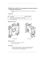
background image

AA7B


5


The amplifier 

On the left side of the circuit you will see J1.  This is where the receiving 
antenna is connected.  The signal(s) picked up by the antenna are 
connected to U1 pin 5 through a .01uF coupling capacitor.  This capacitor is 
necessary to isolate U1 from any DC levels that might be present at J1 and 
allow the AC, in this case RF signals, to enter the AA7B.  U1 is an electronic 
relay.  This device is really neat in that it performs like the old fashioned big 
mechanical relays of yester-year.  This relay will switch signals from DC to 
over 3GHz very effectively.  They are NOT a power relay capable of 
controlling large amounts of power -- instead it is used for very small levels, 
like the ones we are dealing with in the AA7B.  You will notice that the 
symbol for U1 looks like a simple Single Poll Double Throw (SPDT) switch 
with a few other connections.  Pins 4 and 6 are the control lines that control 
the relay and also supply operating power.  These two pins are connected so 
that when one is in a low state the other is high.  For example when pin 6 is 
high pin 4 is low and the signal is connected from pin 5 to pin 1.  We’ll talk 
more about this later.  For now we’ll assume this is the case and follow the 
signal through the AA7B.  
 
From U1 pin 1 the signal goes through C3, another coupling capacitor, to Pin 
4 of Q3.  Q3 is an N-Channel MOSFET Tetrode transistor.  If you’re familiar 
with older components, it’s just a solid state version of a tetrode vacuum 
tube.  Pin 4, ‘G1’, is one of the gate terminals .  The small ac voltage (signal)  
applied to this gate controls the large (compared to the input signal) current 
that flows from the source terminal, ’S’, to drain terminal, ‘D’.  As the 
changing (AC) drain current flows through L1 and R7 a signal or voltage is 
developed that has the same characteristics as the gate signal except 
opposite phase and greater amplitude.  That is how the device amplifies.    
 
Pin 3, ‘G2’,  is another gate and is between ‘G1’ and the ‘D’ to ‘S.’  By 
applying a DC level to ‘G2’ the amount of ‘G1’s’ signal that is allowed to 
control the output current ‘D’ to ‘S’ is changed.  Think of it as the volume 
control on your stereo.  This control is provided by the voltage divider R2 
(front panel Gain control), R3 and R4.    When the user adjusts R2 so that 
the arrow, called a wiper, on R2 moves toward R3 the voltage applied to ‘G2’ 
is increased.  Increasing the voltage on ‘G2’ allows more of the signal on G1 
to control the output current increasing Q3’s gain.  By adjusting R2 so that 
the wiper moves toward R4 the voltage on ‘G2’ decreases, decreasing the 
gain of Q3.  Notice that the voltage on R2’s wiper is applied to Q3 through 
R5 and Q2 through R10.  This allows the user to control the gain of both 
amplifiers simultaneously. 
 
C7 is another coupling capacitor which couples the amplified signal from the 
drain terminal of Q3 to the ‘G1’ terminal of Q2.  Looking at Q2 and the 
components around it you will see that it is almost identical to the Q3 circuit.  
The output signal from Q2’s drain terminal is the amplified RF signal applied 

Summary of Contents for AA7B

Page 1: ...used with existing antenna Clear concise assembly instructions carefully guide you to a finished kit that works FIRST time Informative manual answers questions on theory hookups and uses enhances resale value too Ideal companion to any Ramsey receiver Power switch cuts the AA7B active antenna in and out of the antenna line with no need to change cables Runs on a standard 9 volt battery or external...

Page 2: ... Detector ML Music Lights Kit RAMSEY AMATEUR RADIO KITS HR Series HF All Mode Receivers QRP Series HF CW Transmitters CW7 CW Keyer QRP Power Amplifiers RAMSEY MINI KITS Many other kits are available for hobby school scouts and just plain FUN New kits are always under development Write or call for our free Ramsey catalog AA7B ACTIVE ANTENNA KIT INSTRUCTION MANUAL Ramsey Electronics publication No M...

Page 3: ... Build Assembly Strategy 8 Schematic Diagram 10 Parts List 12 Assembly Instructions 13 Initial Tests 15 Using your AA7B 15 Troubleshooting Guide 16 A Final Suggestion 17 Specifications 18 Ramsey Kit Warranty 19 KIT ASSEMBLY AND INSTRUCTION MANUAL FOR RAMSEY ELECTRONICS LLC 590 Fishers Station Drive Victor New York 14564 Phone 585 924 4560 Fax 585 924 4555 www ramseykits com ...

Page 4: ...e negative terminal of the 9 Volt battery is removed from the circuit and power from the external supply will be connected to VR1 This is done to protect the battery from being damaged i e blowing up catching fire etc by applying power from an external source NEVER attempt to charge a non rechargeable battery NEVER attempt to charge a rechargeable battery without the proper charging system If the ...

Page 5: ...nts it s just a solid state version of a tetrode vacuum tube Pin 4 G1 is one of the gate terminals The small ac voltage signal applied to this gate controls the large compared to the input signal current that flows from the source terminal S to drain terminal D As the changing AC drain current flows through L1 and R7 a signal or voltage is developed that has the same characteristics as the gate si...

Page 6: ... have undesirable effects on the circuit operation and will cause it not to work under the right conditions The amplifier bypass circuit If you look below Q3 on the diagram you will see U2 A and U2 B These are CMOS 74HC00 logic NAND gates Without going into the NAND gate operation just know that if a low signal is applied to the input U2 A pins 1 and 2 the output pin 3 will be high In other words ...

Page 7: ...AA7B 7 Rev 1 2 Ramsey Electronics LLC Active Antenna AA7B PARTS LAYOUT DIAGRAM ...

Page 8: ...ron The finished joint should look like a tepee Mount all electrical parts on the top side of the board provided unless other wise directed The top side has the silk screen of the parts with their reference designations When parts are installed the part is placed flat to the board and the leads are bent on the backside of the board to prevent the part from falling out before soldering 1 The part i...

Page 9: ...ode bands electrolytic capacitor polarity transistor shapes dotted or notched ends of IC s and so forth 4 Solder all connections unless directed otherwise Use enough heat and solder flow for clean shiny completed connections Trim or Nip all excess wires extending beyond each solder connection taking care that wire trimmings do not become lodged in PC board solder connections For more information o...

Page 10: ...iometer R2 marked 104 SEMICONDUCTORS 2 BF2040 N Channel MOSFET Tetrode Transistor Q2 Q3 pre mounted 1 LM2936Z 5 0 Voltage Regulator VR1 1 74HC00N CMOS Quad NAND Gate IC U2 2 HMC221 Electronic Relay U1 U5 pre mounted CONTROLS AND HARDWARE 1 DPDT push switch S1 2 PCB mounted BNC jacks J1 J2 1 PCB mounted Power jack J3 1 9 volt battery hold down clamp 1 9 volt battery snap connector BAT1 1 LED power ...

Page 11: ...at the bottom left of the board install J1 the RF input jack Solder all 4 points of the jack securely 2 Install C1 01µF marked 01 103 or 10nF above J1 and below U1 3 Install C3 01µF marked 01 103 or 10nF on the other side of U1 4 Install R1 100k ohm brown black yellow near C3 5 Install C4 01µF marked 01 103 or 10nF next to R1 6 Install R5 10k ohm brown black orange above and to the left of R1 7 In...

Page 12: ...and the black wire denotes the negative hole 27 Install C16 10 µF above U2 Note that electrolytic capacitors have polarity and must be installed properly The negative side of the capacitor is marked with a stripe with negative signs The PC board or the parts layout diagram will show the correctly labeled sign next to the positive hole Be sure to use the correct polarity 28 Install C5 10 µF to the ...

Page 13: ...ceiver as well as an optional add on antenna Testing the AA7B consists of turning it on using it and checking that all of its described features are operational You will need to become accustomed to the signal strength in the highest range of the gain control If you experience any problems consult the Troubleshooting Hints section USING YOUR AA7B For some of our kits this USING section becomes the...

Page 14: ...voltage of the external supply or battery being used 2 Verify the output lead of VR1 is at 5 volts DC If it is not check the input lead of VR1for supplied voltage If input lead is good check installation of VR1 3 Check U2 pin 2 for 5 Volts with the switch in the on position pressed If no 5 volts is present check installation of S1 and U2 LED Not lit have gain 1 Check D1 and R11 for proper installa...

Page 15: ...heck R2 for open or short There are some characteristics associated with preamplifiers and active antennas which do NOT mean that your AA7B is malfunctioning Strong AC hum The antenna is too close to an AC cord or power line and or the RF gain is set too high Unusual oscillations in receiver Some portable receivers not enclosed in metal cases may break into oscillation when connected to any RF pre...

Page 16: ...ck Type BNC Max Signal 0 dBm 1mW Power Supply Requirements Jack Type 2 1mm center External Supply Voltage 9 to 20 VDC External Supply Current 40mA max Internal Battery Voltage 9 Volt Battery Internal Battery Current 40mA max Circuit Board Dimensions 4 in X 4 75 in 101 6mm X 120 4mm Case Dimensions 5 in X 5 25 in X 1 5 in 127mm X 113 4mm X 38 1mm Weight completed with 9V alkaline Approx 10 4oz 294 ...

Page 17: ...actory for a full refund less shipping The return package should be packed securely Insurance and tracking is highly recommended A reminder this applies to unassembled kits They must be in the same new condition as received not partially assembled Assembled kits cannot be returned for credit No RMA s are required simply return to Ramsey Electronics LLC Attn Product Returns 590 Fishers Station Driv...

Page 18: ...embly and Instruction manual for RAMSEY MODEL NO AA7B ACTIVE ANTENNA KIT REQUIRED TOOLS Soldering Iron Thin Rosin Core Solder Needle Nose Pliers Small Diagonal Cutters ADDITIONAL SUGGESTED ITEMS Helping Hands Holder for PC Board Parts Desoldering Braid TOTAL SOLDER POINTS 101 ESTIMATED ASSEMBLY TIME Beginner 3 hr Intermediate 2 hr Advanced 45 min RAMSEY ELECTRONICS LLC 590 Fishers Station Drive Vi...

Reviews: