Rabbit 3000 User Manual Download Page 206

198

Rabbit 3000 Microprocessor

When the spectrum spreader is engaged, the frequency is modulated, and individual clock 
cycles may be shortened or lengthened by an amount that depends on whether the clock 
doubler is engaged and whether the spectrum spreader is set to the normal or strong set-
ting. The frequency modulation amplitude and the change in clock cycle length is greater 
at lower voltages or higher temperatures since it is sensitive to process parameters. The 
spectrum spreader also introduces a time offset in the system clock edge and an equal off-
set in edges generated relative to the system clock. A feedback system limits the worst 
case time error of any signal edge derived from the system clock to plus or minus 20 ns for 
the normal setting and plus or minus 40 ns for the strong setting at 3.3 V. The maximum 
time offset is inversely proportional to operating voltage. The time error will not usually 
interfere with communications channels, except perhaps at the extreme upper data rates. 
More details on dealing with the clock variation introduced are available elsewhere (see 
Chapter 16, “AC Timing Specifications”).

If the input oscillator frequency is 4 MHz or less the spectrum spreader modulation of fre-
quency will enter the audio range of 20 kHz or less and may generate an audible whistle in 
FM stations. For this reason it may be desirable to disable the spreader for low speed oscil-
lators (where it is probably unnecessary anyway). However, in practical cases the whistle 
may not be audible due to the very low level of the interference from a system with low 
oscillator frequency and the spectrum spreader engaged. Each halving of clock frequency 
reduces the amplitude of the harmonics at a given frequency by 6 dB or more.

The effect of pure harmonic noise on an FM station is to either completely block out a sta-
tion near the harmonic frequency or to disturb reception of that station. If the spectrum 
spreader is engaged then interference will be spread across the band but will generally be 

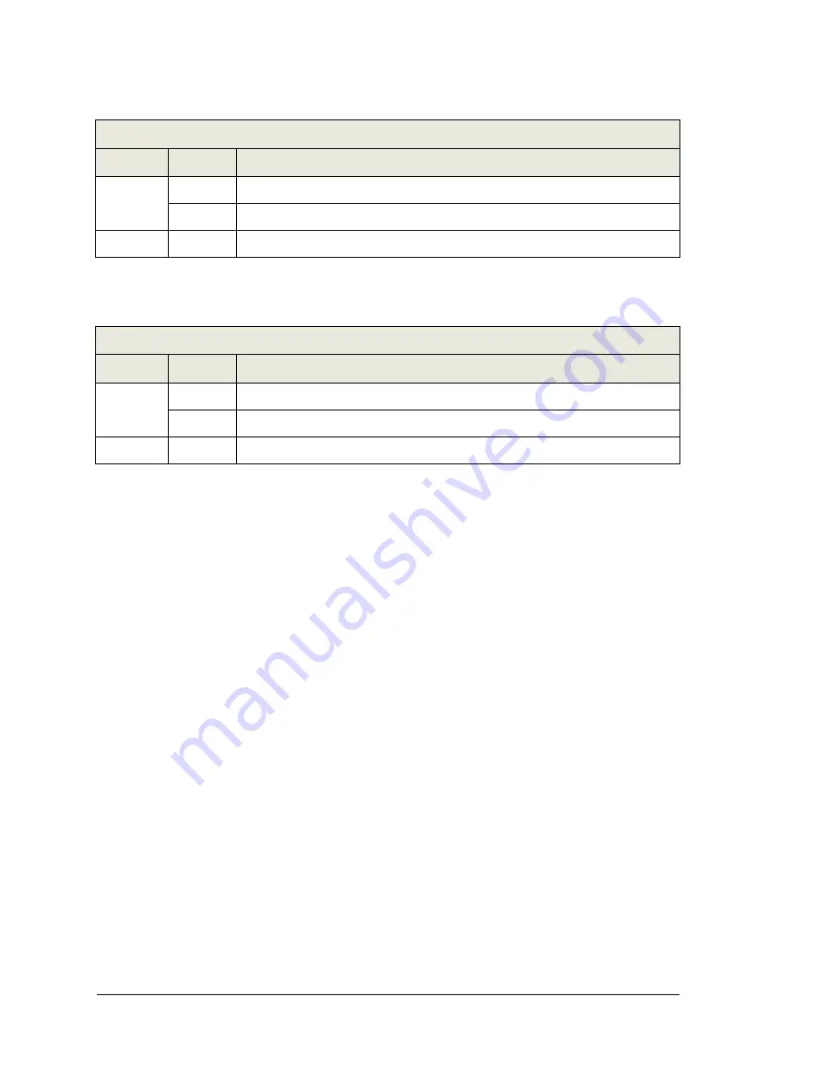
Table 15-1.  Spread Spectrum Enable/Disable Register

Global Clock Modulator 0 Register

(GCM0R)

(Address = 0x0A)

Bit(s)

Value

Description

7

0

Enable normal spectrum spreading.

1

Enable strong spectrum spreading.

6:0

These bits are reserved.

Table 15-2.  Spread Spectrum Mode Select

Global Clock Modulator 1 Register

(GCM1R)

(Address = 0x0B)

Bit(s)

Value

Description

7

0

Disable the spectrum spreader. 

1

Enable the spectrum spreader.

6:0

These bits are reserved.

Summary of Contents for 3000

Page 1: ...Rabbit 3000 Microprocessor User s Manual 019 0108 020426 A...

Page 2: ...it Semiconductor reserves the right to make changes and improvements to its products without providing notice Trademarks Rabbit 3000 is a trademark of Rabbit Semiconductor Dynamic C is a registered tr...

Page 3: ...t 18 2 3 2 Standard BIOS 19 2 4 Dynamic C Support for the Rabbit 19 Chapter 3 Details on Rabbit Microprocessor Features 21 3 1 Processor Registers 21 3 2 Memory Mapping 23 3 2 1 Extended Code Space 26...

Page 4: ...ns 62 5 6 DC Characteristics 64 5 6 1 3 3 Volts 64 5 7 I O Buffer Sourcing and Sinking Limit 64 Chapter 6 Rabbit Internal I O Registers 65 6 1 Default Values for all the Peripheral Control Registers 6...

Page 5: ...l Timing With Internal Clock 167 12 7 2 Clocked Serial Timing with External Clock 167 12 8 Synchronous Communications on Ports E and F 169 12 9 Serial Port Software Suggestions 173 12 9 1 Controlling...

Page 6: ...Writing I O Registers 226 18 2 1 Using Assembly Language 226 18 2 2 Using Library Functions 226 18 3 Shadow Registers 227 18 3 1 Updating Shadow Registers 227 18 3 2 Interrupt While Updating Register...

Page 7: ...ter 21 Instructions in Alphabetical Order With Binary Encoding 245 Appendix A 253 A 1 The Rabbit Programming Port 253 A 2 Use of the Programming Port as a Diagnostic Setup Port 254 A 3 Alternate Progr...

Page 8: ...Rabbit 3000 Microprocessor...

Page 9: ...language development system Dynamic C Z World is providing the soft ware development tools for the Rabbit 3000 The Rabbit 3000 is easy to use Hardware and software interfaces are as uncluttered and ar...

Page 10: ...ry chips such as RAM and flash memory connect directly to the microprocessor with no glue logic A memory access time of 55 ns suffices to support up to a 30 MHz clock with no wait states with a 30 ns...

Page 11: ...8 bit registers 3 for each direction of communication Independent strobes and interrupts are used to control the slave port in both directions Only a Rabbit and a RAM chip are needed to construct a c...

Page 12: ...e cur rent is proportional to voltage and clock speed at 1 8 V and 3 84 MHz the current would be about 5 mA and at 1 MHz the current is reduced to about 1 mA To allow extreme low power operation there...

Page 13: ...2 CS1 CS0 OE1 OE0 WE1 WE0 PA 7 0 PB 7 0 PC 7 0 PD 7 0 PE 7 0 TXA RXA CLKA ATXA ARXA TXB RXB CLKB ATXB ARXB TXC RXC CLKC TXD RXD CLKD ADDRESS BUS 8 bits RESOUT PF 7 0 PG 7 0 Asynch Serial Synch Serial...

Page 14: ...used to create an intelligent peripheral or a slave processor For example protocol stacks can be off loaded to a Rabbit slave The master can be any processor The Rabbit can be cold booted so unprogram...

Page 15: ...5 mm LQFP 10 x 10 x 1 2 mm TFBGA 24 18 x 3 mm PQFP Spacing between package pins 0 4 mm 16 mils LQFP 0 8 mm TFBGA 0 65 mm 26 mils PQFP Separate power and ground for I O buffers EMI reduction Yes No Clo...

Page 16: ...t 3000 Microprocessor Serial ports with support for SDLC HDLC IrDA communications 2 None Maximum asynchronous baud rate clock speed 8 clock speed 32 Input capture unit 2 None Feature Rabbit 3000 Rabbi...

Page 17: ...This is because the price of static memory has decreased to the point that it has become the preferred choice for medium scale embedded systems The Rabbit has no support for DMA direct memory access b...

Page 18: ...ndingly reduced using built in hardware resulting in low power consumption by the memories The Rabbit external bus uses 2 clocks for read cycles and 3 clocks for write cycles This has many advantages...

Page 19: ...e above 8 V The 5 V tolerant feature allows 5 V devices that have a suitable switching threshold to be directly connected to the Rabbit This includes HCT family parts operated at 5 V that have an inpu...

Page 20: ...lock with the internal clock The clocked serial mode may be used to support SPI bus devices Serial Port A has special features It can be used to cold boot the system after reset Serial Port A is the n...

Page 21: ...use an interrupt that can be used to set up the next bit to be output on the next timer pulse This feature can be used to generate precisely controlled pulses whose edges are positioned with high accu...

Page 22: ...t Figure 2 3 Slave Port Data Paths The slave Rabbit can read the same registers as I O registers When incoming data bits are written into one of the registers status bits indicate which registers have...

Page 23: ...ry bus is relieved of the capacitive load that would otherwise slow the memory For core modules based on the Rabbit 3000 fewer pins are required to exit the core module since the slave port and the I...

Page 24: ...re recognized a start condition and a stop condition The start condition may be used to start counting and the stop condition to stop counting However the counter may also run continuously or run unti...

Page 25: ...Once the phase relationship is known between the counters it is then possible to output pulses a precise time delay after an input pulse is captured provided that the time delay is great enough for th...

Page 26: ...I O ring The I O ring located on the 4 edges of the die holds the bonding pads and the large transistors used to create the I O buffers that drive signals to the external world The core section inside...

Page 27: ...and provides basic services for software run ning on the Rabbit 2 4 Dynamic C Support for the Rabbit Dynamic C is Z World s interactive C language development system Dynamic C runs on a PC under Windo...

Page 28: ...20 Rabbit 3000 Microprocessor...

Page 29: ...ition in the instruction set as the Z80 R register but its function is to point to an interrupt vector table for internally generated interrupts Figure 3 1 Rabbit Registers A F H L D E B C IX IY SP PC...

Page 30: ...The addressing range is expanded by means of the memory mapping hardware see Memory Mapping on page 23 and by special instructions For most embedded applications 64K of data mem ory as opposed to cod...

Page 31: ...resses The processor except for certain LDP instructions sees only a 16 bit address space That is it sees 65536 distinctly addressable bytes that its instructions can manipulate Three segment register...

Page 32: ...startup code as well as other code that may happen to be stored there The data segment usage varies depending on the overall strategy for setting up memory It may be an extension of 10000 E000 D000 7...

Page 33: ...orrespond to the normal control lines found on static mem ory chips chip select or CS output enable or OE and write enable or WE In order to generate these memory control signals the 20 bit address sp...

Page 34: ...nstructions mod ify both the program counter PC and the XPC register causing the XPC window to point to a different part of memory where the target of the long jump call or return is located The XPC s...

Page 35: ...ll require at least 12K of root code This amount of data space is sufficient for many embedded applications One approach to getting more data space is to place data in RAM or in flash memory that is n...

Page 36: ...into a single root code segment In the D space the segments are separately mapped to flash and RAM to provide storage for con stant data and variable data The hardware method to achieve separate 20 bi...

Page 37: ...accessed one at a time rather than randomly between all the groupings An example would be the software structures associated with a TCP IP communication protocol connection where the same code accesse...

Page 38: ...aced using CS0 and one RAM memory chip interfaced using CS1 The smallest practical amount of flash is 128K and the smallest practical amount of RAM is 32K Smaller chips could be sup ported but such sm...

Page 39: ...hen each task requires its own stack Since the stack has its own segment in 16 bit address space it is easy to use available RAM memory to support a large number of stacks When a pre emptive change of...

Page 40: ...cks for each byte of the op code and for each data byte read Three clocks are needed for each data byte written One additional clock is required if a memory address needs to be computed or an index re...

Page 41: ...d Immediate Data to a Register A constant that follows the op code in the instruction stream can generally be loaded to any register except PC IP and F Load to the PC is a jump instruction This includ...

Page 42: ...gisters above or an immediate data byte LD HL r not a legal instruction LD r IX d r is any of 7 registers d is 128 to 127 offset LD r IX d same but alternate destination LD IX d r r is any of 7 regist...

Page 43: ...any of HL DE BC 2 bytes 4 clocks LD dd DE LD IX HL LD IY HL LD HL IY LD HL IX LD SP HL 1 byte 2 clocks LD SP IX LD SP IY Other 16 bit register moves can be constructed by using 2 byte moves 3 3 5 Regi...

Page 44: ...re ww is HL DE BC SP ADC HL ww ADD and ADD carry SBC HL ww sub and sub carry INC ww increment the register without affecting flags In the above op codes IX or IY can be substituted for HL The ADD and...

Page 45: ...n HL SBC HL HL sets HL 0 if C 0 sets HL 0ffffh if C 1 BOOL HL HL 1 if C was set otherwise HL 0 convert not carry bit into boolean variable in HL SBC HL HL HL 0 if C 0 else HL ffff if C 1 INC HL HL 1 i...

Page 46: ...LD DE n2 LD A b save sign of BC MUL form product in HL BC OR a test sign of BC multiplier JR p x1 if plus continue ADD HL DE adjust for negative sign in BC x1 RL DE test sign of DE JR nc x2 if not ne...

Page 47: ...O address specified by the 16 bit memory address used For example IOI LD A 85h loads A register with contents of internal I O register at location 85h LD IY 4000h IOE LD HL IY 5 get word from externa...

Page 48: ...HL 2 EXX 2 EX DE HL 2 Move between IX IY and DE DE IX IY DE DE IX IY IX IX DE EX DE HL LD HL IX IY LD IX IY HL EX DE HL 8 clocks total DE IX IY EX DE HL LD IX IY HL EX DE HL 8 clocks total 3 4 3 Mani...

Page 49: ...these operations can be performed as follows assuming that the object is to set HL to 1 or 0 depending on whether the compare is true or false compute HL DE unsigned integers EX DE HL uncomment for DE...

Page 50: ...no carry HL B B is constant not zero LD DE 65535 B ADD HL DE C if HL B CCF C if true SBC HL HL if C 1 else 0 INC HL 16 clocks 1 if true else 0 HL B B is zero true if HL 0 BOOL HL result in HL HL B and...

Page 51: ...re 3 8 Mapping Signed Integers to Unsigned Integers by Inverting Bit 15 3 4 5 Atomic Moves from Memory to I O Space To avoid disabling interrupts while copying a shadow register to its target register...

Page 52: ...nes do not affect the XPC interrupt routines must be located in the root code space However they can jump to the extended code space after saving the XPC on the stack 3 5 1 Interrupt Priority The Z80...

Page 53: ...ations The effect of the processor priority on interrupts is shown in Table 3 1 The priority of the interrupt is usually established by bits in an I O control register associated with the hard ware th...

Page 54: ...equest lines for the separate devices before they are or ed together The interrupt dis patcher calls the interrupt routines for all devices requesting interrupts in priority order so that all interrup...

Page 55: ...not have an embed ded critical section If this code is nested there is the danger of overflowing the IP register A different version that can be nested is the following PUSH IP IPSET 1 save previous p...

Page 56: ...c a JP HL In this case A has the new XPC and HL has the new PC This code should normally be executed in the root segment so as not to pull the memory out from under the JP HL instruction A call to a c...

Page 57: ...e priority of the interrupt and the amount of time that other interrupt routines of the same or higher priority inhibit interrupts The first instruc tion of the interrupt routine will start executing...

Page 58: ...in the range of 1 256 Timer B can count as fast as 10 MHz with a 20 MHz system clock allowing events to be separated by as little as 100 ns Timer B and the match registers have 10 bits Using Timer B o...

Page 59: ...gure 4 2 A row is driven low then the col umns are scanned for a low input line which indicates a key is closed This is repeated for each row The advantage of using open drain outputs is that if two k...

Page 60: ...e to either memory or to internal I O space The high bit of the address is set to specify the I O space and thus writes are limited to the first 32K of either space The cold boot is terminated by a st...

Page 61: ...lso can do a write to the status register which is used as a signaling device and does not actually write to the status register The three registers that the master can write appear as read reg isters...

Page 62: ...interrupt driven trans fer will be on the order of 100 clocks per byte transferred assuming a 20 instruction inter rupt routine To keep the interrupt routine to 20 instructions the interrupt routine...

Page 63: ...D PC1 RXD VSSCORE VDDCORE PC2 TXC PC3 RXC PAC4 TXB PC5 RXB PC6 TXA PC7 RXA VDDIO VSSIO PF7 AQD2A PWM3 PF6 AQD2B PWM2 PF5 AQD1A PWM1 PF4 AQD1B PWM0 PB7 IA5 SLAVEATTN PB6 IA4 PB5 IA3 SA1 PB4 IA2 SA0 PB3...

Page 64: ...s of the Rabbit 3000 LQFP package Figure 5 2 Mechanical Dimensions Rabbit LQFP Package 14 00 0 10 mm 16 00 0 25 mm 0 10 mm 0 15 mm 0 60 0 18 0 05 mm 0 40 mm 14 00 0 10 mm 16 00 0 25 mm 1 00 mm The sam...

Page 65: ...9 Figure 5 3 PC Board Land Pattern for Rabbit 3000 128 pin LQFP 13 75 mm 16 85 mm 12 4 mm 15 3 mm 0 18 0 05 mm 0 40 mm 13 75 mm 16 85 mm 12 4 mm 15 3 mm 1 55 mm JT 0 29 0 55 mm Toe Fillet JH 0 29 0 60...

Page 66: ...PB5 PB1 XTALA1 PA5 PA1 PF2 WE1 A19 STATUS OE0 A10 PB7 PB4 PB0 VSSIO PA4 PA0 VDDIO VSSIO OE1 CS0 VDDCORE VSSCORE D7 PB3 VDDIO PA7 PA3 A11 A9 A8 A13 D6 D5 D4 D3 A17 VDDCORE VSSCORE A14 D2 VSSIO VDDIO D...

Page 67: ...ADDR 19 0 Output Address Bus various DATA 7 0 Bidirectional Data Bus 19 18 15 10 Status Control WDTOUT Output WDT Time Out 43 STATUS Output Instruction Fetch First Byte 4 SMODE 1 0 Input Bootstrap Mo...

Page 68: ...124 127 PG 7 0 Input Output I O Port G 63 60 38 36 Power processor core VDDCORE 3 3V 8 24 72 88 Power Processor I O Ring VDDIO 3 3V 1 17 33 65 81 97 115 Power Battery Backup VBAT 3 3V or battery 47 G...

Page 69: ...accessed Output enable and write enable are always delayed by one clock from the time the final stable address and chip select are enabled Normally the false memory access attempts to start another in...

Page 70: ...0 PB 7 SLAVE_ATTNB IOAddr 5 PB 6 IOAddr 4 PB 5 IOAddr 3 SLAVE_AD 1 PB 4 IOAddr 2 SLAVE_AD 0 PB 3 IOAddr 1 SLAVE_RDB PB 2 IOAddr 0 SLAVE_WRB PB 1 CLKA CLKA PB 0 CLKB CLKB PC 7 n a RXA yes PC 6 TXA n a...

Page 71: ...PF 6 PWM 2 QRD2_Q PF 5 PWM 1 QRD1_I yes PF 4 PWM 0 QRD1_Q PF 3 QRD2_I yes PF 2 QRD2_Q PF 1 CLKC QRD1_I CLKC yes PF 0 CLKD QRD1_Q CLKD PG 7 RXE yes PG 6 TXE PG 5 RCLKE RCLKE yes PG 4 TCLKE TCLKE PG 3...

Page 72: ...the Rabbit I O buffers are capable of sourcing and sinking 6 mA preliminary of current per pin at full AC switching speed The limits are related to the maximum sustained current permitted by the meta...

Page 73: ...User s Manual 65 6 RABBIT INTERNAL I O REGISTERS...

Page 74: ...0h Parallel Port D No interrupts Parallel Port E No interrupts External I O Control No interrupts Pulse Width Modulator No interrupts Quadrature Decoder IIR 7 1 1 90h External Interrupts INT0 EIR 00h...

Page 75: ...Register GOCR 0x0E W 00000000 MMU Instruction Data Register MMIDR 0x10 R W 00000000 MMU Common Base Register STACKSEG 0x11 R W 00000000 MMU Bank Base Register DATASEG 0x12 R W 00000000 MMU Common Bank...

Page 76: ...W xxxxxxxx Port D Bit 3 Register PDB3R 0x6B W xxxxxxxx Port D Bit 4 Register PDB4R 0x6C W xxxxxxxx Port D Bit 5 Register PDB5R 0x6D W xxxxxxxx Port D Bit 6 Register PDB6R 0x6E W xxxxxxxx Port D Bit 7...

Page 77: ...0 Input Capture Source 1 Register ICS1R 0x59 W xxxxxxxx Input Capture LSB 1 Register ICL1R 0x5A R xxxxxxxx Input Capture MSB 1 Register ICM1R 0x5B R xxxxxxxx Input Capture Trigger 2 Register ICT2R 0x5...

Page 78: ...TC2R 0x04 R xxxxxxxx Real Time Clock Byte 3 Register RTC3R 0x05 R xxxxxxxx Real Time Clock Byte 4 Register RTC4R 0x06 R xxxxxxxx Real Time Clock Byte 5 Register RTC5R 0x07 R xxxxxxxx Timer A Control S...

Page 79: ...rt A Extended Register SAER 0xC5 W 00000000 Serial Port B Data Register SBDR 0xD0 R W xxxxxxxx Serial Port B Address Register SBAR 0xD1 W xxxxxxxx Serial Port B Long Stop Register SBLR 0xD2 W xxxxxxxx...

Page 80: ...E Control Register SECR 0xCC W xx000000 Serial Port E Extended Register SEER 0xCD W 000x000x Serial Port F Data Register SFDR 0xD8 R W xxxxxxxx Serial Port F Address Register SFAR 0xD9 W xxxxxxxx Seri...

Page 81: ...oscillator circuit There are limitations on how low the oper ating power can be due to the requirement that the oscillator and time date clock share the same power pin making it impossible to restric...

Page 82: ...clock peripheral clock Note peripherals cannot be clocked slower than processor external to Rabbit f 2 f 1 f 1 2 4 8 16 divider Reference design for 32 768 kHz oscillator enb internal to Rabbit clock...

Page 83: ...errupt to be pending 4 2 xxx See table below for decode of this field 1 0 00 Periodic interrupts are disabled 01 Periodic interrupts use Interrupt Priority 1 10 Periodic interrupts use Interrupt Prior...

Page 84: ...The values increase or decrease by 1 for each 5 C increase or decrease in temperature The doubled clock is created by xor ing the delayed and inverted clock with itself If the original clock does not...

Page 85: ...of the clock are the memory and I O write pulses and the early option memory output enable The spectrum spreader either stretches or shrinks the low plateau of the clock by a maxi mum of 3 ns for the...

Page 86: ...to the clock frequency and for this reason power can be reduced by slowing the clock when less computing activity is taking place The clock doubler provides a convenient method of temporarily speedin...

Page 87: ...a greater effect in reducing the peak spectral strength as shown in the figure below Figure 7 3 Reduction in Peak Spectral Strength from Spectrum Spreader In the normal spectrum spreading mode the ma...

Page 88: ...one wait state and the clock is divided by 6 then the memory bus cycle will be 18 undivided clocks long and the duty cycle will be 2 18 1 9 with the short chip select option enabled When the 32 768 kH...

Page 89: ...nd should not be used 100 296nS self timed chip selects 192nS best case 457nS worst case 101 234nS self timed chip selects 151nS best case 360nS worst case 110 171nS self timed chip selects 111nS best...

Page 90: ...000 Microprocessor Figure 7 4 Short Chip Select Memory Read Figure 7 5 Self Timed Chip Select Memory Read Cycle clock ADDR DATA T1 T2 Valid MEMOExB MEMCSxB 32KHz ADDR DATA T1 T2 Valid Valid MEMOExB ME...

Page 91: ...vided by 2 10 CLK pin is low 11 CLK pin is high 5 4 00 STATUS pin is active low during a first opcode byte fetch 01 STATUS pin is active low during an interrupt acknowledge 10 STATUS pin is low 11 STA...

Page 92: ...p is powered down This design makes battery backup possible Since the processor operates on a different clock than the RTC there is the possibility of performing a transfer to the holding registers wh...

Page 93: ...RTC counter disable the byte increment function or cancel the RTC reset command except code 80h 40h Arm RTC for a reset with code 80h or reset and byte increment function with code 0c0h 80h Resets all...

Page 94: ...throughout his program because such instructions can become part of an endless loop if the program crashes and thus disable the recovery ability given by having a watch dog The following is a suggest...

Page 95: ...checksums If these go wrong go into an endless loop with interrupts off Table 7 8 Watchdog Timer Test Register WDTTR adr 09h Bit s Value Description 7 0 51h Clock the least significant byte of the WDT...

Page 96: ...mpedance during reset and during power down when only VBAT is pow ered to allow an external RAM connected to CS1 to be powered by VBAT This is possi ble because the CS1 pin is powered by VBAT In this...

Page 97: ...e table for very small interrupt routines Interrupts have priority 1 2 or 3 The processor operates at priority 0 1 2 or 3 If an inter rupt is being requested and its priority is higher than the priori...

Page 98: ...coder Read the status from the QDSR Timer B Read the status from the TBSR Timer A Read the status from the TASR Input Capture Read the status from the ICCSR Slave Port Rd Read the data from the SPD0R...

Page 99: ...processor priority then there will be only one interrupt for the two edges detected The interrupt service routine can read the interrupt pins via Parallel Port E and determine which lines experienced...

Page 100: ...rocessor that it is requesting an interrupt A separate signal line is needed for each device so that the proces sor can determine which devices are requesting an interrupt The following code shows how...

Page 101: ...tes and bytes must be transferred often enough to prevent the watchdog timer from timing out Bootstrap operation is terminated when the SMODE pins are set to zero The SMODE pins are sampled just prior...

Page 102: ...ter the reset ends and the bootstrap mode begins TXA will be low reflecting its function as a parallel port output bit that is cleared by the reset This may be interpreted as a break signal by some se...

Page 103: ...g this value in each quadrant To get the exact High time the Pulse Width Modulator uses the two LSBs of the pulse width register to modify the High time in each quadrant according to the table below T...

Page 104: ...6 counts 64 counts 64 counts 64 counts 64 counts 65 counts 64 counts 64 counts 64 counts n 257 spread 65 counts 64 counts 65 counts 64 counts n 258 spread 65 counts 65 counts 65 counts 64 counts n 259...

Page 105: ...condition and the Stop condi tion Each of these two inputs can be programmed to come from one of four bits bits 1 3 5 or 7 in Parallel Port C D F or G The two inputs can come from the same or differe...

Page 106: ...inputs for the Start and Stop condition allows time delay measurements between two signals This is the mode to use for high speed pulse measurement because only one count latch is available and it ma...

Page 107: ...ing the disable state The operation of the counter as a function of the I and Q inputs is shown below The Quadrature decoders are clocked by the output of Timer A10 giving a maximum clock rate of one...

Page 108: ...crements from FFh to 00h or when the counter decrements from 00h to FFh The timing for the interrupt is shown below Note that the status bits in the QDSR are set coincident with the interrupt and the...

Page 109: ...ttery backing of static RAM When the processor power is removed but battery power is supplied to the battery power pin VBAT CS1 is held in a high impedance state This allows a pull up resistor to the...

Page 110: ...102 Rabbit 3000 Microprocessor Figure 8 2 Typical Memory Chip Connection Rabbit 3000 data lines 8 address Lines 20 CS WE OE CS0 CS1 CS2 OE0 OE1 WE0 WE1 static memory CS WE OE static memory flash RAM...

Page 111: ...nd thus vanish from the memory map The four segments are shown in the example in Figure 8 4 The segment size register SEGSIZE determines the boundaries marked in the diagram The extended code seg ment...

Page 112: ...create a 20 bit address Wraparound occurs if the addition would result in an address that does not fit in 20 bits Table 8 1 Segment Registers Segment Register Function XPC Locates extended code segme...

Page 113: ...patched to the memory chips connected to the Rabbit There are three separate chip select output lines CS0 CS1 and CS2 that can be used to select one of three different memory chips A field in the cont...

Page 114: ...ages of 256K each There is no effect outside the quadrant that the memory bank control register is controlling Table 8 3 Memory Bank Control Register x MBxCR 14h x Memory Bank x Control Register MB0CR...

Page 115: ...ms that are pushing the access time of battery backed RAM By enabling CS1 the delay time of the switch that forces CS1 high when power is off can be bypassed This feature increases power consumption s...

Page 116: ...Value Description 7 3 These bits are ignored for write and return zeros when read 2 0 0xx Normal operation 100 For an XPC access use MB0CR independent of A19 A18 101 For an XPC access use MB1CR indep...

Page 117: ...starts above the root code and data Allocation normally con tinues to the end of the flash memory Data variables are allocated to RAM working backwards in memory Allocation normally starts at 52K in...

Page 118: ...s inversion occurs after the quadrant has been selected The inversion of A19 or A16 controlled by the MMIDR register on D space accesses is used to separate I and D space to different memory locations...

Page 119: ...ive size of the 2 parts depends on the lower 4 bits of the SEG SIZE register which defines the 4k page boundary between the root segment and the data segment Figure 8 5 Combined versus Separate I D Sp...

Page 120: ...ss these regardless of the state of the user program The Dynamic C debugger vari ables are kept at the top of the data segment starting at 52k and working down in memory The user program variables are...

Page 121: ...ith The 16 bit PC controls the address of the instruction usually in the region E000 to FFFF The advantage of paged access is that most instructions continue to use 16 bit addressing Only when an out...

Page 122: ...114 Rabbit 3000 Microprocessor...

Page 123: ...rol for pulse gen eration Port E All bits of Port E can be configured as I O strobes 4 bits of port E can be used as external interrupt inputs One bit of port E is shared with the slave port chip sele...

Page 124: ...an output store 084h in SPCR Parallel Port A is set up as an input port on reset When the port is read the value read reflects the voltages on the pins 1 for high and 0 for low This could be differen...

Page 125: ...PB6 and PB7 this signal is on the signaling lines from the slave port logic Regardless of whether the slave port is enabled PB0 reflects the input of the pin unless Serial Port B has its internal cloc...

Page 126: ...icated outputs as serial port outputs When serving as serial inputs the data lines can still be read from the Parallel Port C data register The parallel port outputs can be selected to be serial port...

Page 127: ...ction register is zeroed making all pins inputs In addition certain bits in the control register are zeroed bits 0 1 4 5 to ensure that data is clocked into the output registers when loaded All other...

Page 128: ...Microprocessor Figure 9 1 Parallel Port D Block Diagram PD7 PD4 I O Data perclk 2 Timer A1 Timer B1 Timer B2 perclk 2 Timer A1 Timer B1 Timer B2 PD3 PD0 ATXA ATXB ARXA ARXB PD5 PD6 inputs Driver opti...

Page 129: ...out dir out dir out dir out PDB0R W adr 068h x x x x x x x PD0 PDB1R W adr 069h x x x x x x PD1 x PDB2R W adr 06Ah x x x x x PD2 x x PDB3R W adr 06Bh x x x x PD3 x x x PDB4R W adr 06Ch x x x PD4 x x...

Page 130: ...e corresponding pin an open drain output if that pin is set up for output Write only PDFR Parallel Port D function control register This port may be used to make port positions 4 and 6 be serial port...

Page 131: ...the port E outputs can be configured as an I O strobe In addition four of the port E lines can be used as interrupt request inputs The output registers are cas caded and timer controlled making it pos...

Page 132: ...are reset to zero On reset the data direction register and function register are zeroed making all pins inputs and disabling the alternate output functions In addition certain bits in the control regi...

Page 133: ...x x PE0 PEB1R W adr 079h x x x x x x PE1 x PEB2R W adr 07Ah x x x x x PE2 x x PEB3R W adr 07Bh x x x x PE3 x x x PEB4R W adr 07Ch x x x PE4 x x x x PEB5R W adr 07Dh x x PE5 x x x x x PEB6R W adr 07Eh...

Page 134: ...used in the clocked serial mode two pins of Parallel Port F are used to carry the serial clock signals When the internal clock is selected in these serial ports the corresponding bit of Parallel Port...

Page 135: ...control register This register is used to control the clocking of the upper and lower nibble of the final output register of the port On reset bits 0 1 4 and 5 are reset to zero On reset the data dir...

Page 136: ...F As inputs Port G can carry the data and clock inputs for these two serial ports The following registers are described in Table 9 17 and in Table 9 18 Table 9 16 Parallel Port G Registers Register N...

Page 137: ...Port F control register This register is used to control the clocking of the upper and lower nibble of the final output register of the port On reset bits 0 1 4 and 5 are reset to zero On reset the d...

Page 138: ...130 Rabbit 3000 Microprocessor...

Page 139: ...the eight I O strobes is active for addresses occupying 1 8th of the 64K external I O address space Figure 10 1 External I O Bus Cycles Table 10 1 shows how the eight I O bank control registers are or...

Page 140: ...es are two clocks long The I O strobes greatly simplify the interfacing of external devices On reset the upper 5 bits of each register are cleared Parallel Port E will not output these signals unless...

Page 141: ...ons but it cannot generate the baud clock Timer B is more flexible when it can be used because the program can read the time from a continu ously running counter and events can be programmed to occur...

Page 142: ...on the negative edge of this pulse When the counter reaches zero the reload register is loaded on the next input pulse instead of a count being performed The reload registers may be reloaded at any t...

Page 143: ...ke place as soon as priorities allow However if the bit is cleared before the interrupt is latched the bit will not cause an interrupt The proper rule to follow is for the interrupt routine to handle...

Page 144: ...2 Timer A Capabilities Timer Cascade Interrupt Dedicated connection A1 none yes Parallel Ports D G Timer B A2 from A1 yes Serial Port E A3 from A1 yes Serial Port F A4 from A1 yes Serial Port A A5 fro...

Page 145: ...as possible and consume minimum power As for general purpose timers Timer A has seven separate subtimer units A1 and A2 A7 that are also referred to as timers Most likely if a serial port is going to...

Page 146: ...e If a periodic clock is desired it is probably not important when the first clock takes place unless a phase relationship is desired relative to a different timers A phase relationship between two ti...

Page 147: ...advanced to the next match register when the match pulse is generated Every time a match condition occurs the processor sets an internal bit that marks the match value in TBLxR as invalid Reading TBCS...

Page 148: ...e clocked parallel ports are being used then a value will normally be loaded into some bits of the parallel port register These bits will become the output bits on the next match pulse It is neces sar...

Page 149: ...gister TBCMR at address 0BEh and the lower 8 bits are in TBCLR at address 0BFh both registers can be read with a single 16 bit I O instruction The following sequence illustrates how the regis ters cou...

Page 150: ...142 Rabbit 3000 Microprocessor...

Page 151: ...ial port signals Table 12 1 Serial Port Signals Serial Port Signal Name Function Serial Port A TXA Serial Transmit Out RXA Serial Transmit In CLKA Clock for clocked mode bidirectional ATXA Alternate s...

Page 152: ...ock RCLKF Optional external receive clock Table 12 1 Serial Port Signals continued Serial Port Signal Name Function Serial Port A Timer A4 Serial Port B Timer A5 TXA RXA TXB RXB CLKA CLKB Input to tim...

Page 153: ...data bits may be transmitted and received in the asynchronous mode The so called 9th bit or address bit mode of operation is also supported The 9th bit can be set high or low by accessing the appropr...

Page 154: ...om the data register LSB first The control regis ter is used to set the transmit and receive parameters The status register may be tested to check on the operation of the serial port Figure 12 2 Funct...

Page 155: ...ers can divide the frequency by any number from 1 to 256 see Chapter 11 The input frequency to the timers can be selected in different ways described in the documentation for the timers One choice is...

Page 156: ...xC5 W 00000000 Table 12 3 Serial Port B Registers Register Name Mnemonic I O Address R W Reset Serial Port B Data Register SBDR 0xD0 R W xxxxxxxx Serial Port B Address Register SBAR 0xD1 W xxxxxxxx Se...

Page 157: ...Port E Data Register SEDR 0xC8 R W xxxxxxxx Serial Port E Address Register SEAR 0xC9 W xxxxxxxx Serial Port E Long Stop Register SELR 0xCA W xxxxxxxx Serial Port E Status Register SESR 0xCB R 0xx00000...

Page 158: ...Description 7 0 Read Returns the contents of the receive buffer In Clocked Serial mode reading the data from this register automatically causes the receiver to start a byte receive operation the curre...

Page 159: ...2 SDLR Address 0xF2 SELR Address 0xCA SFLR Address 0xDA Bit s Value Description 7 0 Read Returns the contents of the receive buffer Write Loads the transmit buffer with an address byte marked with a o...

Page 160: ...eceive buffer was not overrun 1 This bit is set if the receiver is overrun This happens if the shift register and the data register are full and a start bit is detected This bit is cleared when the re...

Page 161: ...e receive buffer was overrun This bit is cleared by reading the receive buffer 4 0 This bit is always zero in clocked serial mode 3 0 The transmit buffer is empty 1 The transmit buffer is not empty Th...

Page 162: ...ffer is empty 1 The transmit buffer is not empty The serial port will request an interrupt when the transmitter takes a byte from the transmit buffer unless the byte is marked as the last in the frame...

Page 163: ...ansmit operation and a byte receive operation simultaneously 5 4 00 Parallel Port C is used for input 01 Parallel Port D is used for input 1x Disable the receiver input 3 2 00 Async mode with 8 bits p...

Page 164: ...art a byte transmit operation and a byte receive operation simultaneously 5 0 Enable the receiver input 1 Disable the receiver input 4 x This bit is ignored 3 2 00 8 bits per character 01 7 bits per c...

Page 165: ...with 8 bits per character 01 Async mode with 7 bits per character In this mode the most significant bit of a byte is ignored for transmit and is always zero in receive data 10 HDLC mode with external...

Page 166: ...xxx These bits are ignored in async mode 4 0 Normal async data encoding 1 Enable RZI coding 3 16ths bit cell IRDA compliant 3 0 Normal Break operation This option should be selected when address bits...

Page 167: ...synchronized clocked serial uses Timer B2 5 4 00 Normal clocked serial clock polarity inactive High Internal or external clock 01 Normal clocked serial clock polarity inactive Low Internal clock only...

Page 168: ...phase Level Manchester data encoding for HDLC receiver and transmitter 110 Biphase Space data encoding for HDLC receiver and transmitter 111 Biphase Mark data encoding for HDLC receiver and transmitte...

Page 169: ...ure 12 3 Generation of Serial Port Interrupts The receive interrupt request flip flop is set after the stop bit is sampled on receive nomi nally 1 2 of the way through the stop bit Data bits are trans...

Page 170: ...ata register empty This causes an interrupt request The interrupt routine normally answers the interrupt before the shift register runs dry 9 to 11 baud clocks depending on the mode of operation The i...

Page 171: ...t if enabled is requested On receive an interrupt is requested when the receiver data register has data This hap pens when data bits are transferred from the receive shift register to the data registe...

Page 172: ...llup resistor is needed on the clock line to prevent spurious clocks while neither party is driving the clock Figure 12 5 Clock Polarities Supported in Clocked Serial Mode In clocked serial mode the s...

Page 173: ...ceive will be initiated without pausing the clock To do this the interrupt has to be ser viced within 1 2 clock To transmit each byte in external clock mode the user must load the data register and th...

Page 174: ...he data rate slows to 40 000 bytes per second If it can answer in 3 5 clocks or 8 75 s the data rate will slow to 36 363 bytes per second and so forth If two way half duplex communication is desired t...

Page 175: ...2 Clocked Serial Timing with External Clock In a system where the Rabbit serial clock is generated by an external device the clock sig nal has to be synchronized with the internal peripheral clock pe...

Page 176: ...with External Clock Mode 00 When clocking the Rabbit externally the maximum serial clock frequency is limited by the amount of time required to synchronize the external clock with the Rabbit perclk If...

Page 177: ...ritten to the address register or long stop register Writing to the address register appends an zero address bit to the data while writing to the long stop register appends an one address bit to the d...

Page 178: ...ing for the data Status bits are buffered along with the data in both receiver and transmitter The receiver automati cally generates an interrupt at the end of a received frame and the transmitter gen...

Page 179: ...a transition occurs earlier or later than expected the count will be modified during the next count cycle If the transition occurs earlier than expected it means that the bit cell boundaries are early...

Page 180: ...etween the sending data rate and the DPLL output clock rate is 1 16 6 With Biphase data encoding the DPLL is designed to work in multiple access conditions where there may not be Flags on an idle line...

Page 181: ...on and immedi ately synchronizes to this transition No clock output is provided to the receiver during the search operation Decoding Biphase Level data requires that the data be sampled at either the...

Page 182: ...circum stances one or more serial ports can be configured to use a higher priority interrupt There is an exception to be aware of when a serial port has to operate at an extremely high speed At 115 20...

Page 183: ...a power of two in length then anding a mask after the increment The actual memory address is the pointer plus a buffer base address 12 9 1 Controlling an RS 485 Driver and Receiver RS 485 uses a half...

Page 184: ...es 12 9 4 Using A Serial Port to Generate a Periodic Interrupt A serial port may be used to generate a periodic interrupt by continuously transmitting characters Since the Tx output via Parallel Port...

Page 185: ...each character for a 9th bit low The 9th bit or parity bit is low if bit 6 of the serial port status register SxSR is set to a 1 after the character is received If the 9th bit is not a zero then the...

Page 186: ...onnected after the address byte Some microprocessor serial ports have a wake up mode of operation In this mode char acters without the 9th bit set to 1 are ignored and no interrupt is generated When t...

Page 187: ...the transmitter and receiver operate at approximately the same baud rate there can be a difference of up to about 5 between their baud rates Thus the receiver full and transmitter empty interrupts wi...

Page 188: ...180 Rabbit 3000 Microprocessor...

Page 189: ...lly it is an independent device that is used to communicate between the two processors A diagram of the slave port is shown in Figure 13 1 Figure 13 1 Rabbit Slave Port The slave port has three data r...

Page 190: ...reg ister is written to and the flag is set to a 0 when the register is read The registers appear to be internal I O registers to the slave To the master at least for a Rabbit master the registers app...

Page 191: ...r Either side that is interrupted can clear the signal that is causing an interrupt request by writ ing to the slave port status register The data bits are ignored but the flip flop that is the source...

Page 192: ...e slaves Each Rabbit in Figure 13 4 has to have RAM memory The master must also have flash memory However the slaves do not need nonvolatile memory since the master can cold boot them over the slave p...

Page 193: ...write requests unless the chip select is low If a Rabbit is used as a master this line can be connected to one of the master s programmable chip select lines I0 I7 SRD Input If SCS is also low this li...

Page 194: ...ed number of lifetime writes to flash memory The slaves reset in Figure 13 4 is under the program control of the master If the master is reset the slave will also be reset because the master s drive o...

Page 195: ...ly if SMODE1 SMODE0 lines are set to 0 1 after the reset ends This features disables the normal operation of the processor and causes commands to be accepted via the slave port register SPD0R These co...

Page 196: ...nvironment is controlled the serial protocol is simpler and faster than if error correction needs to be taken into account 13 3 1 Slave Applications Motion Controller Many types of motion control requ...

Page 197: ...lave response to each character If the master is to be interrupted to acknowledge each character the slave can create an interrupt in the master by storing a dummy character in SPD0R to cre ate a mast...

Page 198: ...the slave writes to SPD0R Typically the slave will write to SPD0R when there is a change of status on one of the serial ports The slave can interrupt the master at any time by storing to SPD0R It wil...

Page 199: ...the startup procedure If the clock is battery backed there will be no startup delay since the oscillator is already oscillating The startup delay may be as much as 5 seconds Crys tals with low series...

Page 200: ...e When this is done the power consumption is decreased dramatically The current consumption is often reduced to the region of 100 A at this clock speed The Rabbit executes about 6 instructions per mil...

Page 201: ...r is measured by using a quasi peak detector in the spectrum analyzer The quasi peak detector has a charge time constant of 1 ms and a discharge time constant of 550 ms In this manner the peak radiate...

Page 202: ...s typically operate at lower frequencies with slower rise times than the core logic Noise on the power supply rails in the I O ring will be passed through the buff ers and appear on the output pins In...

Page 203: ...re most troublesome for creating unintentional radiation are generally frequencies in the range of 100 300 MHz Lower frequencies are more easily attenuated by decoupling capacitors and do not radiate...

Page 204: ...ar the package or at least minimizing the load capac tance This will reduce the current switched at the clock frequency or at 1 2 the clock fre quency Of course a series resistor will slow rise time p...

Page 205: ...nic The spectrum spreader not only reduces the EMI measured in government tests but it will also often reduce the interference cre ated for radio and television reception The spectrum spreader has thr...

Page 206: ...ns If the input oscillator frequency is 4 MHz or less the spectrum spreader modulation of fre quency will enter the audio range of 20 kHz or less and may generate an audible whistle in FM stations For...

Page 207: ...ect of a pure harmonic on TV reception is to create a herringbone pattern created by a harmonic falling within the station s band If the spreader is engaged the pattern will disappear unless the stati...

Page 208: ...200 Rabbit 3000 Microprocessor...

Page 209: ...bbit 3000 are output synchronized with the internal clock The internal clock is closely synchronized with the external clock CLK that may be optionally output from pin 2 of the TQFP package The delay...

Page 210: ...ve The shortening takes place by shortening the high part of the clock If the doubler is not enabled then every clock is shortened during the low part of the clock period The maxi mum shortening for a...

Page 211: ...ocks per bus cycle plus any wait states that might be specified Figure 16 2 Memory Read and Write Cycles Tadr Tadr Memory Read no wait states CLK A 19 0 Memory Write no extra wait states CLK A 19 0 va...

Page 212: ...ys were measured See Table 16 2 for delays at other voltages Table 16 3 Memory Read Time Delays Time Delay Output Capacitance 30 pF 60 pF 90 pF Clock to address delay Tadr 6 ns 8 ns 11 ns Clock to mem...

Page 213: ...no extra wait states CLK A 15 0 External I O Write no extra wait states CLK A 15 0 IORD valid T1 Tw T1 Tw T2 valid T2 BUFEN IOCSx IOWR BUFEN D 7 0 valid Tsetup Thold CSx IOCSx TCSx TIOCSx TIORD TBUFE...

Page 214: ...ges Table 16 5 I O Read Time Delays Time Delay Output Capacitance 30 pF 60 pF 90 pF Clock to address delay Tadr 6 ns 8 ns 11 ns Clock to memory chip select delay TCSx 6 ns 8 ns 11 ns Clock to I O chip...

Page 215: ...to the clock spectrum spreader from 2T Example clock 29 49 MHz T 34 ns operating voltage is 3 3 V bus loading is 60 pF address to output time 8 ns see Table 16 2 data setup time 1 ns the spectrum spr...

Page 216: ...ubject to variation arising from process variation operating voltage and temperature Minimum and maximum clock low times for various doubler settings are given in the formulas and in the graph below M...

Page 217: ...the asymmetery of the original oscillator clock Example Clock 29 49 MHz T 34 ns operating voltage is 3 3 V the clock doubler has a nominal delay of 16 ns resulting in a minimum clock low time of 12 8...

Page 218: ...um spreader is enabled clock periods are shortened by a small amount depending on whether the normal or the strong spreader setting is used and depending on the operating voltage If the clock doubler...

Page 219: ...llator delayed and inverted Doubled clock Delay time 48 52 P 0 48P 0 52P 0 48P 0 52P Data out Example Write Cycle write pulse early write pulse option Example Read Cycle Address CS Address CS output e...

Page 220: ...assumed for cal culating the current consumption estimates below A crystal frequency of 3 6864 MHz is a good choice for a low power system consuming between 2 and 18 mA at 3 3 V as the clock frequency...

Page 221: ...ure 16 8 Rabbit 3000 System Current vs Frequency at 3 3 V 0 5 10 15 20 25 30 35 40 0 2 4 6 8 10 12 14 16 Clock Frequency MHz I mA xtal 25 80 xtal 14 74 xtal 11 05 xtal 3 68 0 20 40 60 80 100 120 0 10...

Page 222: ...mption consists of the processor core the external recom mended external tiny logic 32 kHz oscillator and the memory The oscillator consumes 17 A at 3 3 V and this drops rapidly to about 2 A at 1 8 V...

Page 223: ...her component and becomes negligible at 1 4 V 3 The current consumed by the built in main oscillator when turned on This current is proportional to Vc above and is equal to 1 mA at 3 3 V 4 The current...

Page 224: ...s given by Itotal 0 32 V f 0 23 Vc f 5 Vc where f is in kHz V is the operating voltage and Vc V V 2 0 7 Leakage the standby current of the reset generator the current consumption of the oscilla tor an...

Page 225: ...elect duty cycle The dynamic part is computed using 0 5 f in mA where f is the bus speed in MHz At 0 46 MHz 3 68 MHz 8 and using a short chip select the duty cycle is about 10 giving a static current...

Page 226: ...V2 0 31 V Generally the oscillator will not start unless the voltage is about 1 4 V However the oscil lator will continue to run until the voltage drops to about 0 8 V If the oscillator stops the curr...

Page 227: ...ure 16 11 Reduced Power External Main Oscillator Table 16 7 lists results for the reduced power external oscillator with no current limiting resistors Design Recommendations Add current limiting resis...

Page 228: ...220 Rabbit 3000 Microprocessor...

Page 229: ...rom the user s application It occupies space at the bot tom of the root code segment When execution of the user s program starts at address zero on power up or reset it starts in the BIOS When Dynamic...

Page 230: ...s possible to substitute a different periodic interrupt This alternative is not supported by Z World since the cost of connecting a crys tal is very small The periodic interrupt keeps the interrupts t...

Page 231: ...virtual watchdogs for other code that must be run periodically If hits to the hardware watchdog are scattered through a program then it may be possible for the code to enter an endless loop where the...

Page 232: ...224 Rabbit 3000 Microprocessor...

Page 233: ...up an endless loop to determine when to exit sleepy mode A routine updateTimers is pro vided to update the system timer variables by directly reading the real time clock and to hit the watchdog while...

Page 234: ...lable to read and write I O registers These functions are pro vided for convenience For speed assembly code is recommended For a complete description of the functions noted in this section refer to th...

Page 235: ...I O register A NULL pointer may replace the pointer to a shadow register as an argument to WrPortI and WrPortE the shadow register associated with the port will not be updated A pointer to the shadow...

Page 236: ...he data bits written are ignored For example a write to the status register in the Rabbit serial ports is used to clear the transmitter interrupt request but the data bits are ignored and the status r...

Page 237: ...ame oscillator as the real time clock there is no relative gain or loss of time between the two A millisecond timer variable MS_TIMER is also maintained by the Virtual Driver Two utility routines are...

Page 238: ...230 Rabbit 3000 Microprocessor...

Page 239: ...age 236 16 bit Arithmetic and Logical Ops on page 236 8 bit Arithmetic and Logical Ops on page 237 8 bit Bit Set Reset and Test on page 238 8 bit Increment and Decrement on page 238 8 bit Fast A regis...

Page 240: ...IOI and IOE affect source S Z L V The L V logical overflow flag serves a dual purpose L V is set to 1 for logical operations if any of the four most significant bits of the result are 1 and L V is res...

Page 241: ...carry 100 LZ logical zero 101 LO logical one 110 P sign plus 111 M sign minus Logical zero if all four of the most significant bits of the result are 0 Logical one if any of the four most significant...

Page 242: ...I S Z V C Operation LD A BC 6 r s A BC LD A DE 6 r s A DE LD BC A 7 d BC A LD DE A 7 d DE A LD HL n 7 d HL n LD HL r 6 d HL r B C D E H L A LD r HL 5 r s r HL LD IX d n 11 d IX d n LD IX d r 10 d IX d...

Page 243: ...a 64K page boundary Since the LDP instruc tion operates on two byte values the second byte will wrap around and be written at the start of the page if you try to read or write across a page boundary T...

Page 244: ...n ADD SP d 4 f SP SP d d 0 to 255 POP IP 7 IP SP SP SP 1 POP IX 9 IXL SP IXH SP 1 SP SP 2 POP IY 9 IYL SP IYH SP 1 SP SP 2 POP zz 7 r zzl SP zzh SP 1 SP SP 2 zz BC DE HL AF PUSH IP 9 SP 1 IP SP SP 1 P...

Page 245: ...DE 4 f L 0 IY IY DE RL DE 2 fr L CY DE DE CY left shift with CF RR DE 2 fr L DE CY CY DE RR HL 2 fr L HL CY CY HL RR IX 4 f L IX CY CY IX RR IY 4 f L IY CY CY IY SBC HL ss 4 fr V HL HL ss CY cout if s...

Page 246: ...instruction output inverted carry C is set if A B if the oper ation or virtual operation is A B Carry is cleared if A B SUB outputs carry in opposite sense from SBC and CP 19 11 8 bit Bit Set Reset an...

Page 247: ...L HL 6 0 HL 7 CY HL 7 RLC IX d 13 f b L IX d IX d 6 0 IX d 7 CY IX d 7 RLC IY d 13 f b L IY d IY d 6 0 IY d 7 CY IY d 7 RLC r 4 fr L r r 6 0 r 7 CY r 7 RR HL 10 f b L HL CY CY HL RR IX d 13 f b L IX d...

Page 248: ...on clk A I S Z V C Operation LDD 10 d DE HL BC BC 1 DE DE 1 HL HL 1 LDDR 6 7i d if BC 0 repeat LDI 10 d DE HL BC BC 1 DE DE 1 HL HL 1 LDIR 6 7i d if BC 0 repeat If any of the block move instructions a...

Page 249: ...mn LRET 13 PCL SP PCH SP 1 XPC SP 2 SP SP 3 RET 8 PCL SP PCH SP 1 SP SP 2 RET f 8 2 if f PCL SP PCH SP 1 SP SP 2 RETI 12 IP SP PCL SP 1 PCH SP 2 SP SP 3 RST v 10 SP 1 PCH SP 2 PCL SP SP 2 PC R v v 10...

Page 250: ...er growing stack RETI pops IP from stack and then pops return address The instruction reti can be used to set both the return address and the IP in a single instruction If preceded by a LD XPC a compl...

Page 251: ...a practical op code The codes that are concerned with decimal arithmetic DAA RRD and RLD could be simulated but the simulation is very inefficient The bit in the status register used for half carry i...

Page 252: ...LD A IIR was I register The following Z80 Z180 instructions have been dropped and are not supported Alterna tive Rabbit instructions are provided Z80 Z180 Instructions Dropped Rabbit Instructions to U...

Page 253: ...affect destination s IOI and IOE affect source S Z L V The L V logical overflow flag serves a dual purpose L V is set to 1 for logical operations if any of the four most signif icant bits of the resul...

Page 254: ...y 011 C carry 100 LZ logical zero 101 LO logical one 110 P sign plus 111 M sign minus Logical zero if all four of the most significant bits of the result are 0 Logical one if any of the four most sign...

Page 255: ...11011101 11011100 4 f L 0 AND IY DE 11111101 11011100 4 f L 0 AND n 11100110 n 4 fr L 0 AND r 10100 r 2 fr L 0 BIT b HL 11001011 01 b 110 7 f s BIT b IX d 11011101 11001011 d 01 b 110 10 f s BIT b IY...

Page 256: ...7 JP mn 11000011 n m 7 JR cc e 001cc000 e 2 5 JR e 00011000 e 2 5 Note If byte following op code is zero next sequential instruction is executed If byte is 2 11111110 jr is to itself LCALL xpc mn 110...

Page 257: ...n 11011101 00101010 n m 13 s LD IX SP n 11011101 11000100 n 11 LD IX HL 11011101 01111101 4 LD IX mn 11011101 00100001 n m 8 LD IY mn 11111101 00101010 n m 13 s LD IY SP n 11111101 11000100 n 11 LD IY...

Page 258: ...011101 11100101 12 PUSH IY 11111101 11100101 12 PUSH zz 11zz0101 10 RES b HL 11001011 10 b 110 10 d RES b IX d 11011101 11001011 d 10 b 110 13 d RES b IY d 11111101 11001011 d 10 b 110 13 d RES b r 11...

Page 259: ...01011 00100110 10 f b L SLA IX d 11011101 11001011 d 00100110 13 f b L SLA IY d 11111101 11001011 d 00100110 13 f b L SLA r 11001011 00100 r 4 fr L SRA HL 11001011 00101110 10 f b L SRA IX d 11011101...

Page 260: ...252 Rabbit 3000 Microprocessor...

Page 261: ...target reset line which should be drivable by an external CMOS driver The STATUS pin is used to by the Rabbit based target to request attention when a breakpoint is encountered in the target under tes...

Page 262: ...needs to begin or to enable the port and wait for interrupts The SMODE pins can be used for signaling and can be detected by a poll However recall that the SMODE pins have a special function after re...

Page 263: ...tions board can accept these unsolicited messages using its clocked serial port To prevent overrunning the receiver the target can wait for a handshake signal on one of the SMODE lines or there can be...

Page 264: ...36 21 1968 46 38 Clock Frequency Crystal Freq MHz Divisor 115200 baud Memory Access Time ns 3 6864 1 8432 4 534 7 3728 3 6864 8 262 14 7456 7 3728 16 127 18 4320 9 2160 20 100 22 1184 11 0592 24 81 29...

Page 265: ...perfect Bugs are always present in a system of any size In order to prevent danger to life or property it is the responsibility of the system designer to incorporate redundant protective mechanisms a...

Page 266: ......

Reviews: