


152
Rabbit 2000 Microprocessor
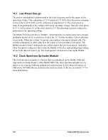
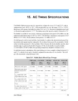
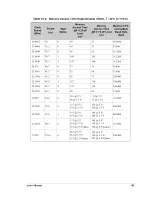
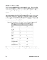
The industrial clock speed values in Table 15-1 (at a maximum temperature of 85°C) are
improved by 7% over commercial ratings at 70°C (which are extended to -40°C here). The
effect of temperature alone is a clock speed that is approximately 1.2% lower for each 5°C
temperature increase. The maximum clock speed is approximately directly proportional to
the operating voltage.
If serial communication is to be used at standard baud rates, then certain clock speeds
must be used. These clock speeds are usually multiples of 1.8432 MHz to ensure that baud
rates of 57,600 bps, 19,200 bps, and less will be available. Multiples of 3.6862 MHz
ensure that baud rates of 115,200 bps, 38,400 bps, and less will be available. Multiples of
1.2288 MHz ensure that baud rates of 38,400 bps and less will be available. The standard
Rabbit BIOS will accept any clock speed that is a multiple of 0.6144 MHz.
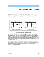
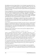
The graphs in Figure 15-1 and Figure 15-2 illustrate the maximum clock speed at which
no failure is detected for a typical Rabbit 2000 as the voltage and temperature are varied.
The official design specifications specify a lower maximum frequency to allow for pro-
cess variation.
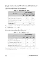
The die suffers significant self-heating at higher clock speeds. The die to ambient thermal
impedance is 44°C/W at zero air flow. At 5 V and a current consumption of 65 mA, this
would result in about 15°C of self-heating, and would reduce the maximum clock speed
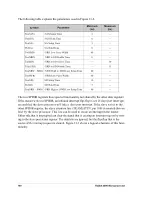
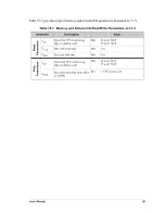
by approximately 3%. This reduction is included in Table 15-2, which provides the mem-
ory access time requirements.
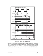
When interfacing to memory devices, the memory access time required for a directly
interfaced memory is given by:
access time = (clock period)*(2 + wait states) - T
setup
- T
adr
(1)
where T
adr
is the delay between the rising edge of T
1
and address valid, and T
setup
is the
data setup time relative to the clock. T
adr
and T
setup
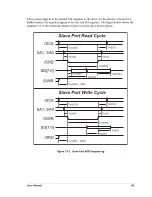
are shown in Figure 15-3 to Figure 15-
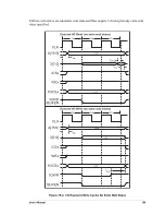
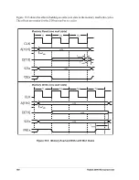
4 for memory read/write and I/O read/write cycles. Most 5 V memories are TTL compatible
in that they switch at 0.8 V and 2.0 V. T
setup
is specified from the point at which the input
voltage reaches 30% or 70% of VDD for falling and rising signals respectively. T
oe
is
specified for the time from the clock that is required for the signal to reach 0.8 V.
The T
adr
measured was the time required for the signal to fall from a high level to 0.8 V.
T
adr
depends on the bus loading—address line A0 has a more powerful driver and can han-
dle double the capacitance with the same delay times. The T
adr
times also apply to the
memory chip select lines.
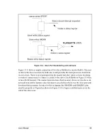
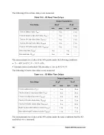
The formula in Equation (1) remains true if the clock doubler is used, except that the
access time must be reduced by 4% of one clock period if there is an odd number of wait
states. The length of the T
oe
pulse is subjected to a reduction of up to 4% if the clock dou-
bler is used.
Summary of Contents for 2000
Page 1: ...Rabbit 2000 Microprocessor User s Manual 019 0069 041018 M...
Page 12: ...6 Rabbit 2000 Microprocessor...
Page 46: ...40 Rabbit 2000 Microprocessor...
Page 54: ...48 Rabbit 2000 Microprocessor...
Page 76: ...70 Rabbit 2000 Microprocessor...
Page 96: ...90 Rabbit 2000 Microprocessor...
Page 142: ...136 Rabbit 2000 Microprocessor...
Page 154: ...148 Rabbit 2000 Microprocessor...
Page 170: ...164 Rabbit 2000 Microprocessor...
Page 174: ...168 Rabbit 2000 Microprocessor...
Page 180: ...174 Rabbit 2000 Microprocessor...
Page 202: ...196 Rabbit 2000 Microprocessor...
Page 206: ...200 Rabbit 2000 Microprocessor...
Page 226: ......
Page 230: ...224 Rabbit 2000 Microprocessor...


