UMTS/HSPA+ Module Series
UC200A-GL_Hardware_Design 27 / 78
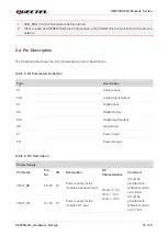
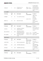
The following table shows the details of power supply and GND pins.
Table 8: Pin Definition of Power Supply
3.4.2. Reference Design for Power Supply
The performance of the module largely depends on the power source. The power supply of the module
should be able to provide sufficient current of 3 A at least. If the voltage drops between input and output
is not too high, it is suggested that an LDO should be used to supply power to the module. If there is a
big voltage difference between input and the desired output VBAT, a buck converter is preferred as the
power supply.
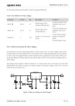
The following figure shows a reference design for +5 V input power source. The design uses the LDO
MIC29302WU from Micrel company. The typical output of the power supply is about 3.8 V and the
maximum load current is 3.0 A.
DC_IN
MIC29302WU
IN
OUT
EN
G
N
D
AD
J
2
4
1
3
5
VBAT
100 nF
470 µF
100 nF
100K
47K
470 µF
330R
51K
1%
1%
4.7K
47K
VBAT_EN
Figure 6: Reference Design of Power Supply
Pin Name
Pin No.
I/O
Description
Comment
VBAT_BB
59, 60
PI
Power supply for the
module’s baseband part
It must be provided with
sufficient current up to
0.8 A.
VBAT_RF
57, 58
PI
Power supply for the
mo
dule’s RF part
It must be provided with
sufficient current up to
1.8 A.
VDD_EXT
7
PO
Provide 1.8 V for external
circuit
It can provide a pull-up
power to the external
GPIO.
If unused, keep it open.

