5G Module Series
RM505Q-AE Hardware Design
RM505Q-AE_Hardware_Design 21 / 79
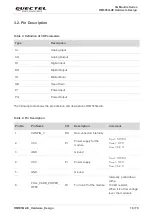
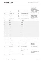
51
GND
Ground
52
PCIE_CLKREQ_N
OD
PCIe clock request.
Open drain
Active LOW.
53
PCIE_REFCLK_M
AI,
AO
PCIe reference clock (-)
100 MHz.
Requires differential
impedance of 85 Ω
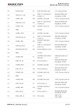
54
PCIE_WAKE_N
OD
PCIe wake up.
Open drain
Active LOW.
55
PCIE_REFCLK_P
AI,
AO
PCIe reference clock (+)
100 MHz.
Requires differential
impedance of 85 Ω
56
RFFE_CLK*
DO
Used for external MIPI IC
control
1.8 V power domain
57
GND
Ground
58
RFFE_DATA*
DO
Used for external MIPI IC
control
1.8 V power domain
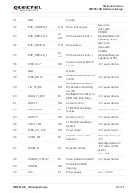
59
LAA_TX_EN*
DO
Notification from SDR to
WLAN when transmitting
via LTE
1.8 V power domain
60
WLAN_TX_EN*
DI
Notification from WLAN to
SDR while transmitting
1.8 V power domain
61
ANTCTL*
DO
Antenna control
1.8 V power domain
62
COEX_RXD*
DI
LTE/WLAN coexistence
receive
1.8 V power domain
63
ANTCTL*
DO
Antenna control
1.8 V power domain
64
COEX_TXD*
DO
LTE/WLAN coexistence
transmit
1.8 V power domain
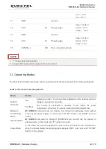
65
RFFE_VIO_1V8
PO
Power output
1.8 V power output
66
USIM1_DET
DI
(U)SIM1 card insertion
detection
Internally pulled up to
1.8 V
67
RESET_N
DI
Reset the module.
Internally pulled up to
1.5 V with a
100 kΩ
resistor
Active LOW.
68
AP2SDX_STATUS*
DI
Status indication from AP
1.8 V power domain
69
CONFIG_1
DO
Connected to GND
internally
70
VCC
PI
Power supply
V
min
= 3.135 V

