5G Module Series
RM505Q-AE Hardware Design
RM505Q-AE_Hardware_Design 20 / 79
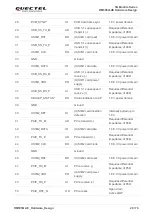
28
PCM_SYNC*
IO
PCM data frame sync
1.8 V power domain
29
USB_SS_TX_M
AO
USB 3.1 super-speed
transmit (-)
Requires differential
impedance of 90 Ω
30
USIM1_RST
DO
(U)SIM1 card reset
1.8/3.0 V power domain
31
USB_SS_TX_P
AO
USB 3.1 super-speed
transmit (+)
Requires differential
impedance of 90 Ω
32
USIM1_CLK
DO
(U)SIM1 card clock
1.8/3.0 V power domain
33
GND
Ground
34
USIM1_DATA
IO
(U)SIM1 card data
1.8/3.0 V power domain
35
USB_SS_RX_M
AI
USB 3.1 super-speed
receive (-)
Requires differential
impedance of 90 Ω
36
USIM1_VDD
PO
(U)SIM1 card power
supply
1.8/3.0 V power domain
37
USB_SS_RX_P
AI
USB 3.1 super-speed
receive (+)
Requires differential
impedance of 90 Ω
38
SDX2AP_STATUS*
DO
Status indication to AP
1.8 V power domain
39
GND
Ground
40
USIM2_DET
DI
(U)SIM2 card insertion
detection
Internally pulled up to
1.8 V
41
PCIE_TX_M
AO
PCIe transmit (-)
Requires differential
impedance of 85 Ω
42
USIM2_DATA
IO
(U)SIM2 card data
1.8/3.0 V power domain
43
PCIE_TX_P
AO
PCIe transmit (+)
Requires differential
impedance of 85 Ω
44
USIM2_CLK
DO
(U)SIM2 card clock
1.8/3.0 V power domain
45
GND
Ground
46
USIM2_RST
DO
(U)SIM2 card reset
1.8/3.0 V power domain
47
PCIE_RX_M
AI
PCIe receive (-)
Requires differential
impedance of 85 Ω
48
USIM2_VDD
PO
(U)SIM2 card power
supply
1.8/3.0 V power domain
49
PCIE_RX_P
AI
PCIe receive (+)
Requires differential
impedance of 85 Ω
50
PCIE_RST_N
OD
PCIe reset.
Open drain
Active LOW.

