


M10 Hardware Design
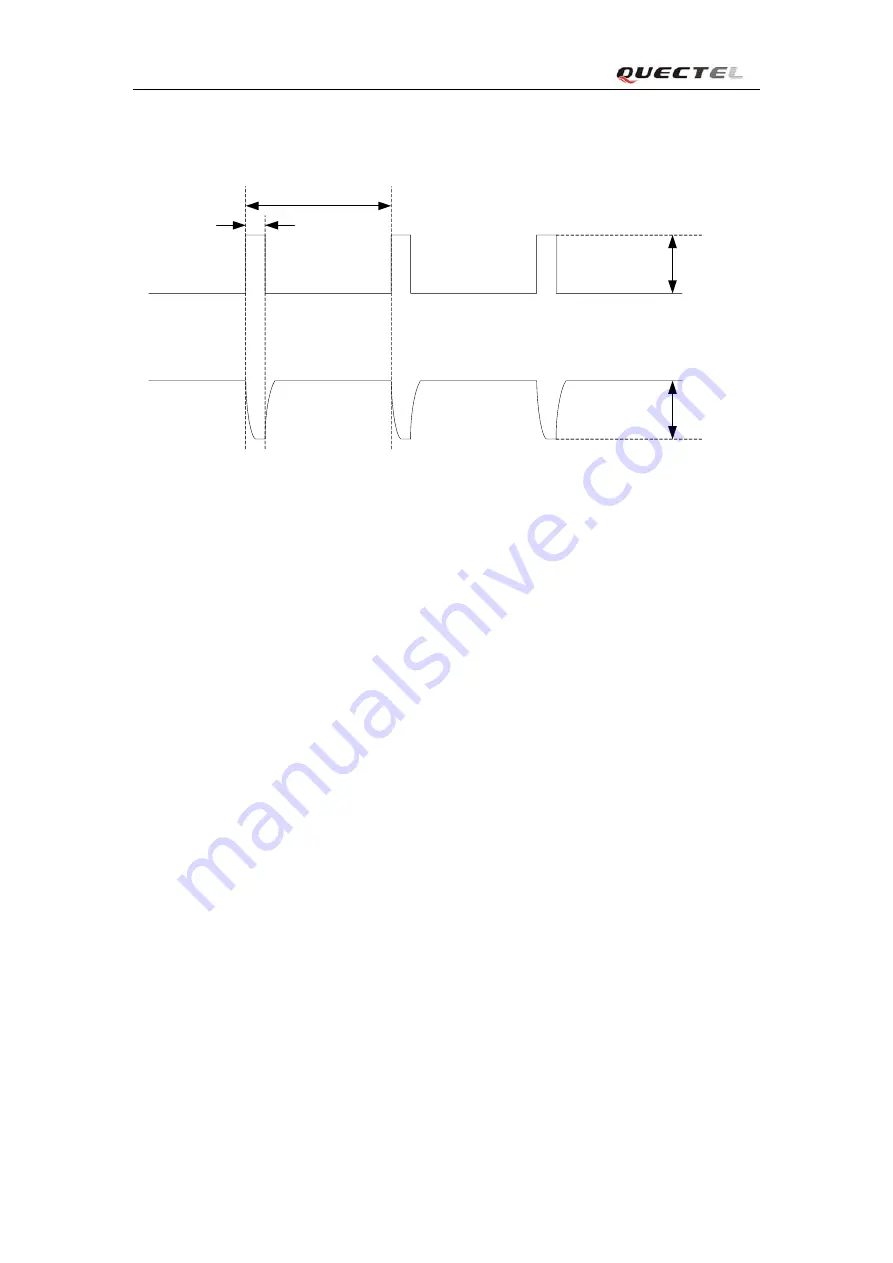
time, around 577us every 4.615ms, in talking mode. The following figure is the VBAT voltage
and current ripple at the maximum power transmitting phase, the test condition is VBAT=4.0V,
VBAT maximum output current =2A, C1=100µF tantalum capacitor (ESR=0.7
Ω
) and C2=1µF.
Max:400mV
Burst:2A
4.615ms
577us
IBAT
VBAT
Figure 4
: Power supply limits during transmitting burst
3.3.1 Power supply pins
The VBAT pins are dedicated to connect the supply voltage; and the GND pins are recommended
for grounding. VRTC pin can be used to back up the RTC.
3.3.2 Minimizing power losses
Please pay special attention to the power supply design for your applications. Please make sure
that the input voltage will never drop below 3.4V even in a transmitting burst during which the
current consumption may rise up to 2A. If the power voltage drops below 3.4V, the module may
be switched off. The PCB traces from the VBAT pads to the power source must be wide enough
to ensure that there isn’t too much voltage drop occur in the transmitting burst mode.
3.3.3 Monitoring power supply
To monitor the supply voltage, you can use the “AT+CBC” command which include three
parameters: charging status, voltage percent and voltage value (in mV). It returns the battery
voltage 1-100 percent of capacity and actual value measured at VBAT and GND.
The voltage is continuously measured at intervals depending on the operating mode. The
displayed voltage (in mV) is averaged over the last measuring period before the “AT+CBC”
command is executed.
For details please refer to
document [1]
M10_HD_V1.00
- 23 -
Quectel


