background image


LTE  Module  Series 

                                                                                                                      EC20  Mini  PCIe  Hardware  Design


EC20_Mini_PCIe_Hardware_Design                    Confidential / Released                                          18 / 36 


3.4. USIM Card Interface 


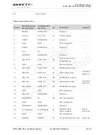
The following table shows the pin definition of the USIM card interface. 


Table 6: USIM Pin Definition 


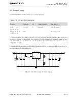
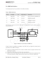
EC20 Mini PCIe supports 1.8V and 3.0V USIM cards. The following figure shows the reference design of 

the 6-pin USIM card.


USIM_VDD

GND

USIM_RST

USIM_CLK

USIM_DATA

22R

22R

22R

100nF

USIM Holder

GND

33pF 33pF 33pF

VCC

RST

CLK

IO

VPP

GND

GND

33pF

15K

Module

USIM_VDD


Figure 4: Reference Circuit of the 6-Pin USIM Card 


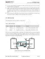
In order to enhance the reliability and availability of the USIM card in your application, please follow the 

criteria below in the USIM circuit design: 


Keep layout of USIM card as close to the module as possible. Assure the length of the trace as less 

than 200mm as possible.   


Keep USIM card signal away from RF and power supply alignment. 


Keep the width of ground and USIM_VDD no less than 0.5mm to maintain the same electric potential. 

The decouple capacitor of USIM_VDD should be less than 1uF and must near to USIM holder. 

Pin No. 

Pin Name


I/O 

Power Domain                         

Description 

8


USIM_VDD


PO                       


1.8V/3.0V                       


Power source for the USIM/SIM card 

10


USIM_DATA


IO


1.8V/3.0V


USIM/SIM data signal 

12


USIM_CLK


DO


1.8V/3.0V


USIM/SIM clock signal 

14


USIM_RST


DO                       


1.8V/3.0V


USIM/SIM reset signal 

Quectel 

Confidential

Summary of Contents for EC20

Page 1: ...EC20 Mini PCIe Hardware Design LTE Module Series Rev EC20_Mini_PCIe_Hardware_Design_V1 0 Date 2015 02 28 www quectel com...

Page 2: ...ORMATION PROVIDED IS BASED UPON CUSTOMERS REQUIREMENTS QUECTEL MAKES EVERY EFFORT TO ENSURE THE QUALITY OF THE INFORMATION IT MAKES AVAILABLE QUECTEL DOES NOT MAKE ANY WARRANTY AS TO THE INFORMATION C...

Page 3: ...EC20 Mini PCIe Hardware Design EC20_Mini_PCIe_Hardware_Design Confidential Released 2 36 About the Document History Revision Date Author Description 1 0 2015 02 28 Radom XIANG Mike ZHANG Initial Quec...
Page 4: ...2 2 Pin Assignment 16 3 3 Power Supply 17 3 4 USIM Card Interface 18 3 5 USB Interface 19 3 6 UART Interface 20 3 7 PCM and I2C Interface 22 3 8 Control Signals 24 3 8 1 RI Signal 25 3 8 2 DTR Signal...

Page 5: ...LTE Module Series EC20 Mini PCIe Hardware Design EC20_Mini_PCIe_Hardware_Design Confidential Released 4 36 5 4 Packaging 34 6 Appendix Reference 35 Quectel Confidential...
Page 6: ...PIN DEFINITION 18 TABLE 7 USB PIN DEFINITION 19 TABLE 8 PIN DEFINITION OF THE UART INTERFACE 20 TABLE 9 PCM AND I2C PIN DEFINITION 22 TABLE 10 CONTROL SIGNAL PIN DEFINITION 24 TABLE 11 RADIO OPERATION...

Page 7: ...LEVEL MATCH CIRCUIT 21 FIGURE 8 TIMING OF PRIMARY MODE 23 FIGURE 9 TIMING OF AUXILIARY MODE 23 FIGURE 10 REFERENCE CIRCUIT OF PCM APPLICATION WITH AUDIO CODEC 24 FIGURE 11 RI BEHAVIOR 25 FIGURE 12 TI...

Page 8: ...interfaces This document can help you to quickly understand the interface specifications electrical and mechanical details and related product information of the EC20 Mini PCIe module To facilitate it...

Page 9: ...less devices on boarding the aircraft if your device offers a Airplane Mode which must be enabled prior to boarding an aircraft Switch off your wireless device when in hospitals or clinics or other he...

Page 10: ...ications EC20 Mini PCIe module can be applied in the following fields PDAs and Laptop Computer Remote Monitor System Vehicle System Wireless POS System Intelligent Meter Reading System Wireless Router...

Page 11: ...Support digital audio2 EC20 A Mini PCIe Support GSM 850 1900MHz Support UMTS B2 B4 B5 Support LTE FDD B2 B4 B5 B12 B17 Support LTE UMTS receive diversity Support GPS GLONASS1 Support digital audio2 F...

Page 12: ...dshake Authentication Protocol usually used for PPP connections SMS Text and PDU mode Point to point MO and MT SMS cell broadcast SMS storage ME by default USIM Interface Support USIM SIM card 1 8V 3...

Page 13: ...N Main Antenna Interface VCC Main Antenna VBAT GNSS Antenna Interface GNSS Antenna Boost Circuit Diversity Antenna Interface Diversity Antenna USIM Holder Optional RI UART DTR Figure 1 Functional Diag...

Page 14: ...wing interface definition and application of EC20 Mini PCIe Power supply USIM interface USB interface UART interface PCM I2C interface Control signals Antenna interface 3 2 EC20 Mini PCIe Interface 3...

Page 15: ...ce for the USIM SIM card 9 GND GND Mini Card ground 10 UIM_DATA USIM_DATA IO USIM SIM data signal 11 REFCLK UART_RX DI UART receive data Connect to DTE s TX 12 UIM_CLK USIM_CLK DO USIM SIM clock signa...

Page 16: ...RESERVED Reserved 34 GND GND Mini Card ground 35 GND GND Mini Card ground 36 USB_D USB_DM IO USB differential data 37 GND GND Mini Card ground 38 USB_D USB_DP IO USB differential data 39 3 3Vaux VCC_...

Page 17: ...0 12 and 14 cannot be used at the same time when using the optional USIM holder 4 means digital audio PCM function is only supported on Telematics version 3 2 2 Pin Assignment The following figure sho...

Page 18: ...rovide enough current and a bypass capacitor of no less than 470 F with low ESR should be used to prevent the voltage from dropping The following figure shows a reference design of power supply The pr...

Page 19: ...he reliability and availability of the USIM card in your application please follow the criteria below in the USIM circuit design Keep layout of USIM card as close to the module as possible Assure the...

Page 20: ...ity when long layout trace and sensitive occasion are applied and should be placed close to the holder 3 5 USB Interface The following table shows the pin definition of USB interface Table 7 USB Pin D...

Page 21: ...tance of ESD component on USB data lines Typically the capacitance value should be less than 2pF There are three preconditions when enabling EC20 Mini PCIe to enter into the sleep mode 1 Execute AT co...

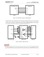
Page 22: ...C must be inserted between module and PC A RS 232 level shifter SN65C3238 provided by Texas Instruments is recommended The following figure shows the reference design of RS232 level match circuit DTR...

Page 23: ...ks as master only In primary mode the data is sampled on the falling edge of the PCM_CLK and transmitted on the rising edge the PCM_SYNC falling edge represents the MSB In this mode PCM_CLK supports 1...

Page 24: ...the PCM_SYNC rising edge represents the MSB In this mode PCM interface operates with a 128kHz PCM_CLK and an 8kHz 50 duty cycle PCM_SYNC only The following figure shows the timing relationship in auxi...

Page 25: ...10 Reference Circuit of PCM Application with Audio Codec 3 8 Control Signals The following table shows the pin definition of control signals Table 10 Control Signal Pin Definition Pin No Pin Name I O...

Page 26: ...low level will wake up the module AT command AT QCFG pwrsavedtr is used to disable the sleep control function 3 8 3 W_DISABLE Signal EC20 Mini PCIe provides W_DISABLE signal to disable wireless commun...

Page 27: ...signal of EC20 Mini PCIe is used to indicate the network status of the module which can absorb the current up to 40mA According to the following circuit in order to reduce the current of the LED a res...

Page 28: ...Rx diversity antenna interface and a GNSS antenna interface All of these connectors are ECT818000117 The following figure shows the overall sizes of RF connector Figure 14 Dimensions of the RF Connec...

Page 29: ...Mini PCIe Power supply requirements IO requirements Current consumption RF characteristics GNSS receiver ESD characteristics 4 2 Power Supply Requirements The input voltage of EC20 Mini PCIe is 3 3V 9...

Page 30: ...The following tables show output power and receiving sensitivity of conducted RF of EC20 Mini PCIe module Table 15 Output Power of Conducted RF Parameter Description Min Max Unit VIH Input High Voltag...

Page 31: ...alcomm GPS and GLONASS and could be used in Qualcomm gpsOneXTRA technology one kind of A GNSS This technology will download XTRA file from the internet server to enhance the TTFF XTRA file contains pr...

Page 32: ...d 31 36 4 6 ESD Characteristics The following table shows characteristics of EC20 Mini PCIe ESD Table 17 ESD Characteristics Part Contact Discharge Air Discharge Unit Power Supply and GND 5 10 kV Ante...

Page 33: ...Dimensions 5 1 General Description This chapter mainly describes the following dimensions of EC20 Mini PCIe Mechanical Dimensions of EC20 Mini PCIe Standard Dimensions of Mini PCI Express Packaging 5...

Page 34: ...sign Confidential Released 33 36 5 3 Standard Dimensions of Mini PCI Express The following figure shows the standard Dimensions of Mini PCI Express Please refer to document 1 for detailed A and B Figu...
Page 35: ...or which compiles with the directives and standards listed in the document 1 The following figure takes the Molex 679100002 as an example Figure 18 Dimensions of the Mini PCI Express Connector Unit mm...

Page 36: ...mmands Manual 3 Quectel_EC20_GNSS_AT_Commands_Manual EC20 GNSS AT Commands Manual Abbreviation Description bps Bits Per Second CS Coding Scheme CS Circuit Switched DC HSPA Dual carrier High Speed Pack...

Page 37: ...uipment Module MIMO Multiple Input Multiple Output MMS Multimedia Messaging Service MO Mobile Originated MT Mobile Terminated PCM Pulse Code Modulation PDU Protocol Data Unit PPP Point to Point Protoc...

Reviews: