
LTE Module Series
EC20 Mini PCIe Hardware Design
EC20_Mini_PCIe_Hardware_Design Confidential / Released 20 / 36
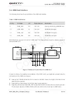
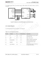
In order to ensure the USB interface design corresponding with the USB 2.0 specification, please comply
with the following principles:
It is important to route the USB signal traces as differential pairs with total grounding. The impedance
of USB differential trace is 90ohm.
Do not route signal traces under crystals, oscillators, magnetic devices and RF signal traces. It is
important to route the USB differential traces in inner-layer with ground shielding, and not only upper
and lower layer but also right and left side should be shielded.
If you use the USB connector, you should keep the ESD components as close to the USB connector
as possible. Pay attention to the influence of junction capacitance of ESD component on USB data
lines. Typically, the capacitance value should be less than 2pF.
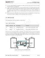
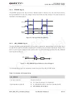
There are three preconditions when enabling EC20 Mini PCIe to enter into the sleep mode:
1. Execute AT command
AT+QSCLK=1
to enable the sleep mode. Refer to
document [2]
.
2. DTR pin should be kept in high level (pull-up internally).
3. USB interface on Mini PCIe must be connected with your USB interface and please guarantee
USB devices are in the suspended state.
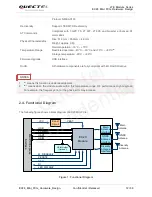
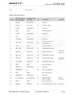
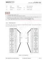
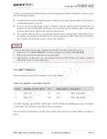
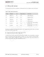
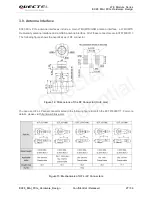
3.6. UART Interface
The following table shows the pin definition of the UART interface.
Table 8: Pin Definition of the UART Interface
The UART interface supports 9600, 19200, 38400, 57600, 115200 and 230400bps baud rate. The default
is 115200bps. This interface can be used for AT communication.
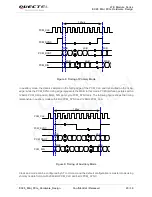
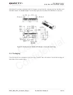
EC20 Mini PCIe is designed as the DCE, and the DCE-DTE connection of UART interface is shown as
below.
Pin No.
EC20 Mini PCIe Pin Name
I/O
Power Domain
Description
11
UART_RX
DI
3.3V
UART receive data
13
UART_TX
DO
3.3V
UART transmit data
NOTES
Quectel
Confidential