background image


                                                 LPWA Module Series


BG95xA-GL&BG950S-GL_TE-B_User_Guide                                                                                21 / 24 


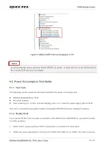
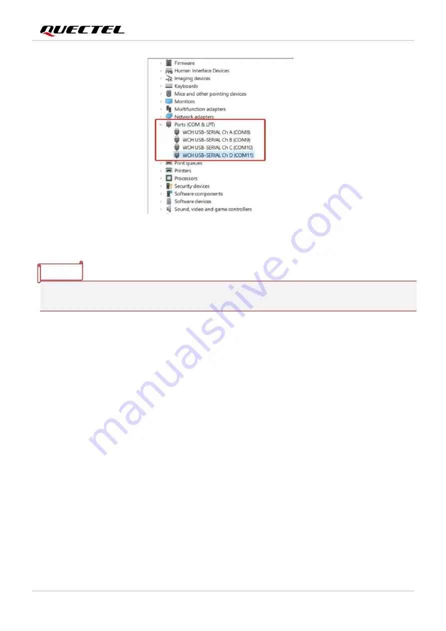
Figure 9: USB-to-UART Interface Displayed on PC 


In  the  procedures  above,  pressing  S0402  (RESET_N  button)  at  least  100  ms  on  the  BG95xA-GL  & 
BG950S-GL TE-B can reset the module. 


4.2. 

Power Consumption Test Guide 

4.2.1. 

Test Tools 

The followings are the equipment and tools needed for the power consumption test: 


BG95xA-GL/BG950S-GL TE-B 


DC power analyzer 


Wire, soldering iron, tin wire, and wire stripping pliers, etc. to weld the power supply cord on TE-B. 


This power consumption test guide is based on Keysight's N6705C DC power analyzer for testing. 

4.2.2. 

Modify TE-B 

If you use the TE-B to test the power consumption of the BG95xA-GL & BG950S-GL, you need to modify 

the TE-B as follows: 


1.  Switch S0201 (power switch) to "OFF" to disconnect the module from other parts. 


2.  Solder two wires respectively to the two pins (VBAT and GND) of the J0202. One wire is used as 

NOTE 

Summary of Contents for BG95 Series

Page 1: ...BG95xA GL BG950S GL TE B User Guide LPWA Module Series Version 1 0 Date 2023 10 20 Status Released...

Page 2: ...h we employ commercially reasonable efforts to provide the best possible experience you hereby acknowledge and agree that this document and related services hereunder are provided to you on an as avai...

Page 3: ...y To implement module functionality certain device data are uploaded to Quectel s or third party s servers including carriers chipset suppliers or customer designated servers Quectel strictly abiding...

Page 4: ...y cause interference on sensitive medical equipment so please be aware of the restrictions on the use of wireless devices when in hospitals clinics or other healthcare facilities Terminals or mobiles...

Page 5: ...e Series BG95xA GL BG950S GL_TE B_User_Guide 4 24 About the Document Revision History Version Date Author Description 2023 07 26 Arvin WU Creation of the document 1 0 2023 10 20 Arvin WU First officia...

Page 6: ...nt 11 2 3 Key Features 14 2 4 Functional Diagram 16 3 Kit Accessories Assembly 17 3 1 Accessories List 17 3 2 Accessories Assembly 18 4 Operation Procedures 19 4 1 Operation Procedure with Single Boar...

Page 7: ...G95xA GL BG950S GL_TE B_User_Guide 6 24 Table Index Table 1 Components Interfaces Information 12 Table 2 Key Features of TE B 14 Table 3 Accessories List 17 Table 4 Related Documents 24 Table 5 Terms...

Page 8: ...ent 11 Figure 4 Bottom Components Interfaces Placement 12 Figure 5 Functional Diagram of TE B 16 Figure 6 TE B Kit Accessories 17 Figure 7 TE B Kit Accessories Assembly 18 Figure 8 Interface Diagram o...

Page 9: ...on details of BG95xA GL and BG950S GL TE B which is an assistant tool for engineers to develop applications and test basic functionalities of Quectel BG950A GL BG951A GL BG952A GL BG953A GL BG955A GL...

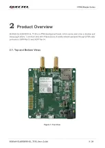
Page 10: ...BG95xA GL BG950S GL TE B is a LPWA development board which can be used alone to develop and debug applications It communicates with infrastructures of mobile network operators through LPWA radio proto...

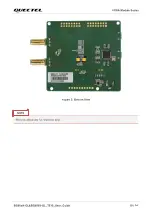
Page 11: ...LPWA Module Series BG95xA GL BG950S GL_TE B_User_Guide 10 24 Figure 2 Bottom View Pictures above are for reference only NOTE...

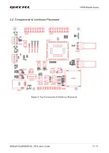
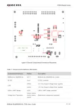
Page 12: ...de 11 24 2 2 Components Interfaces Placement J0401 J0301 U0203 U0202 J0201 S0201 J0202 U0601 J0603 J0604 J0602 J0601 J0502 J0501 S0404 J0402 S0402 S0401 S0405 S0101 U0101 S0102 D0403 D0404 D0405 D0406...

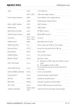
Page 13: ...rfaces Information Components Interfaces RefDes Description BG95xA GL BG950S GL U0101 BG95xA GL BG950S GL module DC DC U0201 DC DC converter LDO U0202 3 3 V low dropout voltage linear regulator U0203...

Page 14: ...itch only for BG951A GL module Recovery Button S0102 Forced into download mode for BB chip Power Switch S0201 Power switch PWRKEY Button S0401 Turn on off the module RESET_N Button S0402 Reset the mod...

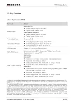
Page 15: ...requirements again 3 BG951A GL only supports one DM UART interface while BG950A GL BG953A GL and BG955A GL support two DM UART interfaces more precisely pin 27 DM_TXD1 and pin 28 DM_RXD1 are connecte...

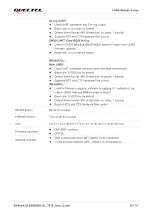
Page 16: ...sion Baud rate 115200 bps by default Default frame format 8N1 8 data bits no parity 1 stop bit Supports RTS and CTS hardware flow control DM UARTs Used for firmware upgrade software debugging RF calib...

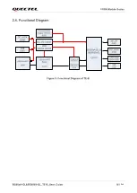
Page 17: ...50S GL U0101 USB to UART J0301 USB to UART Bridge U0301 DC DC U0201 USIM eSIM J0604 U0601 ANT_RF J0501 Voltage level Translators U0302 U0303 U0304 U0305 U0306 LDO U0202 U0203 DC JACK J0201 ANT_GNSS J0...

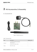
Page 18: ...Guide 17 24 3 Kit Accessories Assembly 3 1 Accessories List Figure 6 TE B Kit Accessories Table 3 Accessories List Item Description Quantity pcs Antenna LTE antenna 699 MHz 2690 MHz SMA J 200 mm 1 Ext...

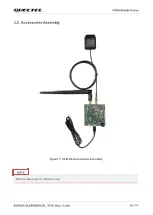
Page 19: ...LPWA Module Series BG95xA GL BG950S GL_TE B_User_Guide 18 24 3 2 Accessories Assembly Figure 7 TE B Kit Accessories Assembly Pictures above are for reference only NOTE...

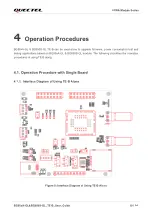
Page 20: ...ne to upgrade firmware power consumption test and debug applications based on BG95xA GL BG950S GL module The following describes the operation procedures of using TE B along 4 1 Operation Procedure wi...

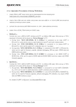
Page 21: ...B COM21 is connected to the debug UART of BG95xA GL which can be used for RF calibration and SFP log output 3 Among them WCH USB SERIAL Ch C COM22 is connected to DM UART of BG95xA GL which can be use...

Page 22: ...ion test BG95xA GL BG950S GL TE B DC power analyzer Wire soldering iron tin wire and wire stripping pliers etc to weld the power supply cord on TE B This power consumption test guide is based on Keysi...

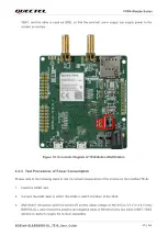
Page 23: ...s of Power Consumption Please refer to the following steps to test the current consumption of the module on the modified TE B 1 Insert the USIM card 2 Connect the USB cable to J0301 the USB to UART in...

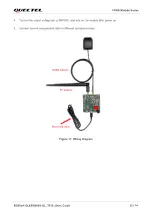
Page 24: ...B_User_Guide 23 24 4 Turn on the output voltage set by N6705C and turn on the module after power up 5 Conduct current consumption tests in different operation modes S0201 J0202 Micro USB cable RF ante...

Page 25: ...3GPP 3rd Generation Partnership Project DC Direct Current DFOTA Delta Firmware Upgrade Over the Air GND Ground GNSS Global Navigation Satellite System LDO Low dropout Regulator LPWA Low Power Wide Are...

Reviews: