QUASAR PROJECT KIT # 3073 - 12/24 HOUR GIANT CLOCK
the displays. This again divided by 500 to obtain a 2Hz
signal which is used to flash the colon on/off. The
seconds display is updated on every second 2Hz signal,
that is, 1Hz.
The RA4 pin on IC1 is set as an output and is used to
discharge the 1n5 capacitor via the 470R resistor.
When RA4 is taken high, its output is open-circuit and
the capacitor charges via the 2K2 resistor and the LDR.
As mentioned above the capacitor charges faster when
the LDR is in bright light (low resistance) and slower
when the LDR is in dull light.The charge time is
monitored by RA4 and used to control the display
dimming.
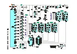
The RB0-RB7 outputs of IC1 drive transistors Q1-Q8
via a 470R base resistor. When the outputs are low, the
transistors are switched on to drive the segments in the
six displays. The segmenta are driven via 82R resistors
while the decimal points are driven via a 180R resistor.
The 0.56” display segments are driven by 220R
resistors.
Different feed resistors are used because the 2.3”
displays have 4 series LEDs per segment and two
series LEDs in the decimal points. The 0.56” displays
only have one LED per segment.
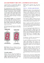
Upside-down Displays.
Normally with multiplexed
displays such as this the same segments for each digit
are connected in parallel. This circuit, however, is
different. Two displays are mounted upside down. This
has been done to obtain a colon between the hours and
minutes and to obtain the am indicator.
The common cathode connections to each display are
driven by IC3, a ULN2003A 7-transistor array. IC3 is
driven via IC2, a 4051 8-channel analog switch or
demultiplexer. In this circuit it has two roles. Firstly, it
acts as a decoder which converts the binary signals on
its three input lines (A, B, C) to drive six outputs, one
for each common cathode LED display. Secondly, it
provides logic level (voltage) translation, changing the
5V signals on its inputs to 12Vsignals to drive IC3. IC2
can do this because it has three supply connections: the
Vdd pin (16) connects to +12V, the Vss pin (8)
connects to the –5V from REG1 (ie, 5V below +12V
supply) and the Vee pin (7) connects to 0V.
As well as acting as the B & C outputs to IC2, pins 17
& 18 of IC1 are monitored via diodes D5 & D6 which
connect to the Minutes and Hours switches resp.The
other side of the switches both connect to the RA3
input (pin 2) of IC1. Normally, pin 2 is held low via the
10K resistor to pin 5. However, if a switch is pressed
and the B or C line driving the switch is high, the RA3
input will also be pulled high. This signals to IC1 that
the switch is pressed. IC1 can determine which switch
is pressed because it ‘knows’ which line (B or C) is
high at the time.
Construction
There are two PCBs. Assemble the components onto
each circuit board according to the overlay. There are
several points to note:
- Links. On 3073B use the four zero ohm resistors
provided. There are 4 on 3073B, not three as I wrote on
the overlay! On 3073A use the tinned copper wire and
cutoff’s from the resistor legs to make the links.
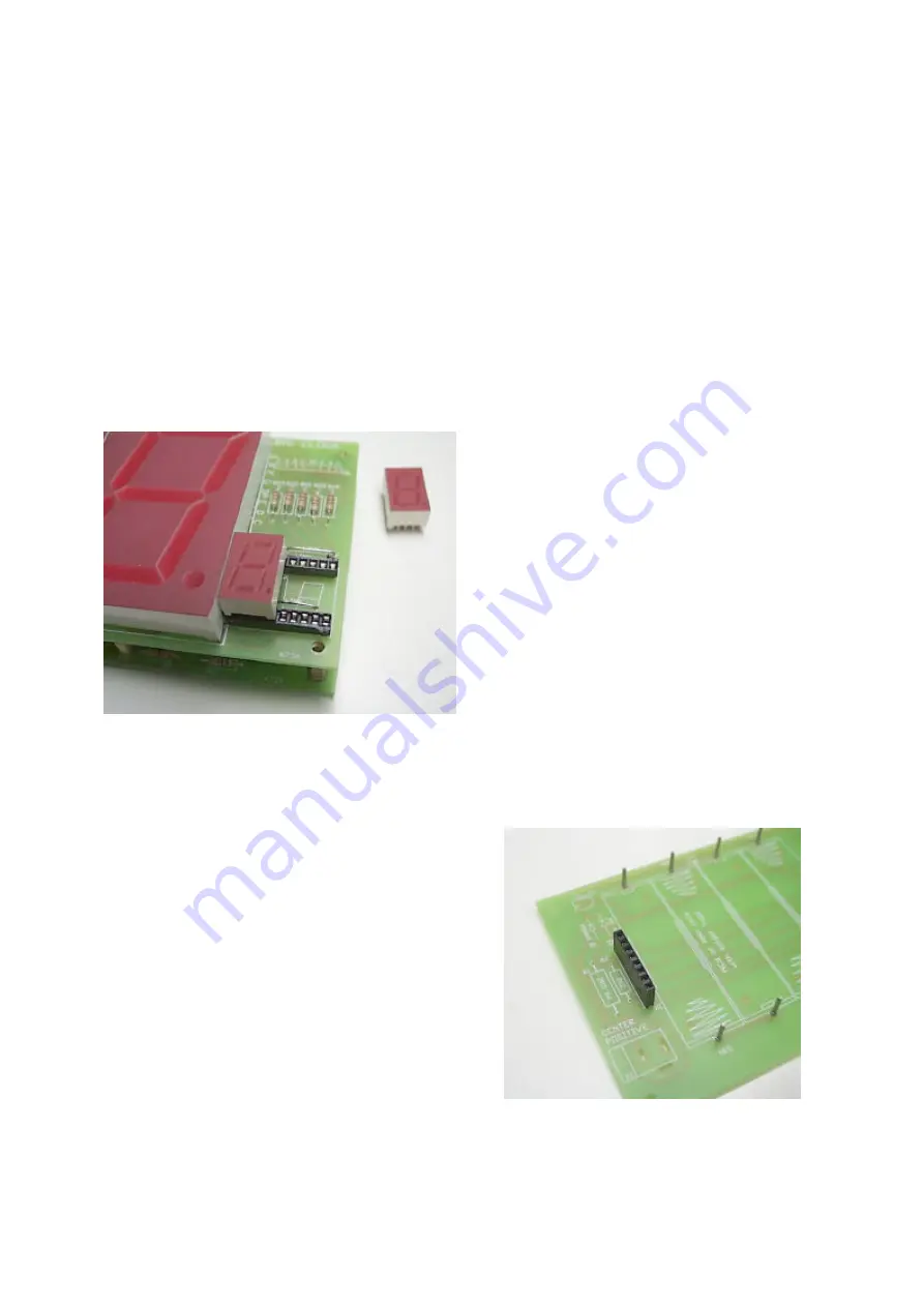
- mount the two 0.56” displays using half of the 20 pin
IC socket.
- two of the 2.3” displays are mounted upside down.
- mount the LDR so its top face is level with the
displays.
If you are going to mount the Clock in a case decide if
you want the two switches S1 and S2 to be higher than
they are.
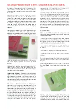
Connecting the Boards.
X1, X2 and X3 on 3073B take
the three
female
8-pin connectors. Solder them into
place.
The three,
male
8-pin connectors X4, X5 and X6 are to
be soldered on the underside of 3073A so that, after
soldering the two boards will fit together both
mechanically and electrically. Note that the connectors
Summary of Contents for 3073
Page 5: ......


