QUASAR PROJECT KIT # 3073 - 12/24 HOUR GIANT CLOCK
a rapid rate that there is no noticeable flicker. When the
displays are driven at full brightness each display is on
for 1/6
th
of the time (the duty cycle is 16.6%.)
The dimming feature uses a 1.5nF capacitor and a
Light Dependent Reststor (LDR.) The capacitor is
discharged each time a digit is about to be lit and the
PIC waits until the capacitor is charged before lighting
the display. In bright light the resistance of the LDR is
low so the capacitor charges up quickly and the display
is lit fast. In darkness or low light the LDR has a much
higher resistance, and the capacitor takes longer to
charge so the duty cycle for each digit is reduced. That
is the display is dimmed. The displays are dimmed
only in clock mode.
Power and Battery Backup.
Use a 12VDC plugpack
for normal operation. Space has been provided for 4 x
AA NiCd or NiMH cells with solder tags. We have
NOT provided these since we think most people will
want to operate the clock with a plugpack. Also
batteries are heavy and add to the kit cost when buyers
may not want them. The metal pins to attach the
batteries to are provided.
With the batteries present when there is a power failure
the seconds hands keeps counting but not the large
displays.
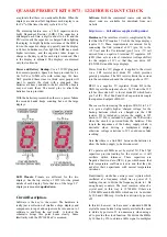
LED Pinouts.
Pinouts are different for the two
displays. See the top overlay of 3073A for the pinout
details of each display. Note that two of the large 2.3”
displays are mounted
upside down.
Circuit Description.
Software is the key to the circuit. The hardware is
really just a collection of interface chips, displays and
components to input and output results into and out of
software to and from the real world. A look at the
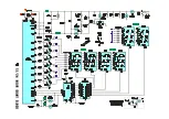
schematic brings this point home clearly. Some
familiarity with the PIC16F84 uC is assumed.
Software.
Both the commented source code and the
object code are available for download from our
website.
http://www.... Full address supplied with product
Hardware.
The interface circuit is complicated by the
fact that the PIC requires 5V while the large displays
require 12V. These requirements are catered for by
connecting the Vdd terminal of IC1 (pin 14) to the
+12V rail and the Vss terminal (pin 5) to a +7V rail
derived from a negative 3-terminal 5V regulator. IC2
(4051) then acts as a level translator (voltage shifter)
for the outputs of IC1 so that they can drive IC3
(ULN2003A) and the large displays.
Power from the 12V plugpack is applied to the circuit
via a 2R2 resistor and diode D1 which provides
polarity protection. The 2R2 resistor limits the current
into the zener diode should the voltage go above 15V.
REG1 is a negative 5V regulator. Diode D2 in the
GND leg sets the output at about –5.6V below the 12V
rail but this extra 0.6V is lost at diode D3 which feeds
pin 5 of IC1. The 100uF and 10uF capacitors decouple
the inputs and outputs of REG1.
The reason for increasing the output of REG1 to 5.6V
is to give a slightly higher ‘charged voltage’ for the
backup batteries which are charged via the 10R
resistor. D3 is included to reduce the supply to IC1
down to 5V. D4 is included to bypass the 10R resistor
when the circuit is powered from the batteries. This
lowers the impedence of the battery supply which is
desirable when driving a multiplexed display,
otherwise voltage variations to IC1 could cause false
resetting.
Note that there is a link LK1 between the batteries to
allow the backup supply to be disconnected.
IC1 operates at 4MHz as set by crystal X1. The 27pF
capacitors provide loading for the crystal so it will
oscillate within tolerance. These capacitors are
Negative Positive Zero (NPO) types which mean that
their temperature coefficient is zero and that they do
not alter their capacitance with normal temperature
variations.
Traditionally, clocks have always used crystals which
oscillated at a frequency which was a power of 2,
making it easier to divide the frequency down to 1 Hz
using bunary counters. The most common value of a
crystal used in this way is 32.768kHz. Others are
3.2768MHz amd 4.096MHz which need to be divided
by 100 and 1000 resp. first before division by powers
of 2.
In this kit, however, we have used a standard 4.0MHz
crystal because beside being readily available the need
to divide by powers of 2 is unnecessary when using a
uC to provide the clock function. We divide the 4MHz
by 16 then by 250 to obtain a 1kHz signal to multiplex
Summary of Contents for 3073
Page 5: ......


