
VISTEK V6333E/D & V6333Q/D
hd/sd sdi digital audio multiplexer
HU-V6333E/D&Q/D
7
2.6
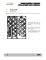
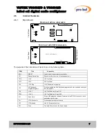
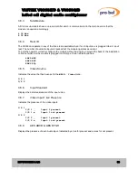
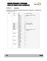
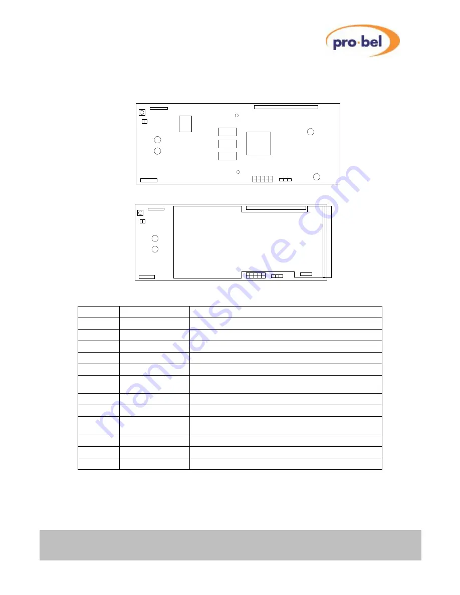
Internal Hardware
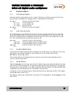
2.6.1
Main Board
Main board with no sub-module
F
ron
t P
an
el
SW1
Flash Card
JP1
JP2
JP3
PL1
M1
TP10
TP17
TP2
TP23
JP4
TP27
TP25
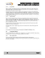
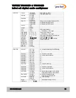
Main board with V6333 sub-module
F
ront
P
a
nel
R
ea
r
C
onne
ct
or
SW1
Flash Card
JP1
JP2
JP3
PL1
FS 1
M1
TP10
TP17
TP23
JP4
V6333 Sub-Module
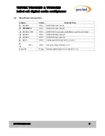
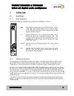
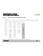
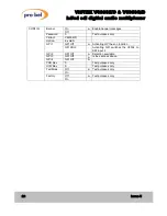
The purposes of the links and switches is shown in the following table.
ITEM
Title
Comments
SW1
RESET
Used to reset the internal microcontroller.
JP1
Debug/Normal Link
Should be left with no link, for development only.
TP10
+1.5V
1V5 Test Point
TP17
+3.3V
3V3 Test Point
JP4
+15V Plug
+15V Alternative supply plug.
JP2
H8 Debug and
Programming Port
For downloading the H8’s Bootloader program, and also used as a serial port
for development.
TP2
+1.8V 1
1V8 Test Point from Reg U301
TP23
+1.8V 2
1V8 Test Point from Reg U309
M1
Flash Card
Stores H8 Application code and Firmware for the FPGA. Also used to store
application specific data.
PL1
JTAG Connector
For development and test use only
JP3
JTAG enable
Link 2-3 for operational use.
FS1
Fuse
The main 2Amp fuse on the frame supply.