background image

PDV-LC10

14

A

B

C

D

1

2

3

4

1

2

3

4

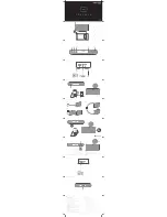
3.2 OVERALL WIRING DIAGRAM

Note : When ordering service parts, be sure to refer to "EXPLODED VIEWS and PARTS LIST" or "PCB PARTS LIST".

VXX2657

VKN1557

VXX2658

VKN1556

ZY, ZL : AC220-230V
              50/60Hz
ZU/CA : AC120V
               60Hz

AC POWER CORD
ZY,ZL : ADG1127
ZU/CA: RDG1034

AC ADAPTER
ZY : VWX1222
ZU/CA: VWX1220
ZL : VXX2696

Summary of Contents for PDV-10

Page 1: ... PIONEER ELECTRONICS ASIACENTRE PTE LTD 253 Allexandra Road 04 01 Singapore 159936 PIONEER CORPORATION 1999 RRV2231 T ZZR OCT 1999 Printed in Japan PDV 10 PORTABLE DVD PLAYER This service manual should be used together with the following manual s Model No Order No Remarks PDV LC10 RRV2212 THIS MANUAL IS APPLICABLE TO THE FOLLOWING MODEL S AND TYPE S ZBW AC230V Adapter ZL AC230V Adapter Type Power ...

Page 2: ...670 Not used Not used P7 7 Protective Tape VEC2073 Not used Not used P7 8 Cushion B VEC1311 Not used Not used P7 9 Cover Plate VNH1056 Not used Not used P7 10 Speaker VVY1002 Not used Not used P7 11 Earth Plate A VBK1091 Not used Not used 7 CONTRAST OF MISCELLANEOUS PARTS PDV 10 ZL PDV 10 ZBW and PDV LC10 ZL are constructed the same except for the following CONTRAST TABLE Part No Remarks PDV LC10 ...

Page 3: ...057 Not used Not used P7 17 Switch Cap VNK4481 Not used Not used P7 18 Flexible Sheet VEC2084 Not used Not used P7 19 F P C 22P VNP1693 Not used Not used P7 20 Rear Cover VNK4484 Not used Not used P7 22 LCD Holder VNK4485 Not used Not used P9 1 Body Assy VXA2375 VXA2377 VXA2377 P9 7 Electrostatic Sheet VEC2082 VEC2121 VEC2121 P9 9 Selector Knob VNK4478 Not used Not used P9 13 Power Knob VNK4477 VN...

Page 4: ... No 5 ZBW Only No 5 ZBW Only No 5 ZBW Only No 1 No 3 Packing Carton Front mark Tray PDV 10 Sheet Insulating Aircap Polyethylene Bag AC Adapter PDV 10 Body No 2 EXTERIOR SECTION Top Cover Body Assy VEB1061 No 6 No 7 Lag Rubber Lag Rubber Lag Rubber Lag Rubber ...

Page 5: ...used C401 C406 VCH1168 Not used C411 C439 CKSRYB473K16 Not used C422 C437 C438 C470 CKSSYB223K16 Not used C413 C418 C419 C421 VCH1174 Not used C412 C440 CKSRYB122K50 Not used C456 CKSSYF103Z50 Not used C467 C468 VCH1169 Not used C628 CKSSYB103K16 CKSSYF103Z50 C855 VCH1175 Not used C858 C859 C877 C882 CKSRYB104K16 Not used R470 R414 RS1 16S1002F Not used R401 R404 R406 R407 R437 R464 RS1 16SS1602F ...

Page 6: ...VIDEO OUT AV IN OUT JACK Tantalum A Tantalum A Tantalum Tantalum A Tantalum Tantalum A Tantalum A Tantalum A Tantalum A Tantalum Tantalum Tantalum Tantalum A from Q858 V V V V V C Y Y Y C V CB F 5 6 PDVDM ASSY 5 6 PDV 10 VWS1408 A 4 6 A 4 6 A 3 6 A 2 6 A 6 6 A 2 6 A 2 6 A 4 6 A V 5DAC VREFA HEAD PHONE VR ...

Page 7: ...5 6 HP OUT JACK Tantalum Tantalum Tantalum Tantalum AUDIO SIGNAL ROUTE ROM DATA SIGNAL ROUTE V CB SIGNAL ROUTE Y SIGNAL ROUTE C SIGNAL ROUTE V CB Y C 2 6 A 4 6 A 2 6 A 2 6 A V5AA VREFA V2R5 V2A The power supply is shown with the marked box ...

Page 8: ...L AC230V Adapter or Battery pack PDV LC10 RRV2212 1 SAFETY INFORMATION 2 2 EXPLODED VIEWS AND PARTS LIST 4 3 BLOCK DIAGRAM AND SCHEMATIC DIAGRAM 12 4 PCB CONNECTION DIAGRAM 31 5 PCB PARTS LIST 38 6 ADJUSTMENT 42 CONTENTS T ZZR SEPT 1999 Printed in Japan THIS MANUAL IS APPLICABLE TO THE FOLLOWING MODEL S AND TYPE S PORTABLE DVD PLAYER Type Power Requirement Remarks Model PDV LC10 DIGITAL OUT OPTICA...

Page 9: ...as Simpson Model 229 2 or equivalent between the earth ground and all exposed metal parts of the appliance input output terminals screwheads metal overlays control shaft etc Plug the AC line cord of the appliance directly into a 120V AC 60 Hz outlet and turn the AC power switch on Any current measured must not exceed 0 5 mA FOR USA MODEL ONLY Also test with plug reversed Using AC adapter plug as r...

Page 10: ...ss S603 is intentionally short circuited in door open state To light the laser in Test mode short circuit S603 Hold S603 in the depressed position from the top as it is a push switch 2 NEVER directly look at the objective lens from a short distance when lighting the laser by short circuiting S603 in door open state CAUTION LASER RADIATION WHEN OPEN AVOID LONG TERM VIEWING OF DIRECT LASER RADIATION...

Page 11: ...ponent parts indicates the importance of the safety factor of the part Therefore when replacing be sure to use parts of identical designation Screws adjacent to mark on the product are used for disassembly Top Rear PDV LC10 Front mark 28 3 2 21 6 4 5 1 23 32 3 31 22 30 20 29 29 19 27 26 10 11 12 13 24 7 8 9 25 Accessory 14 15 24 25 18 16 17 16 6 3 ZU CA ZY Only 3 ZY Only ZU CA Only 33 ...

Page 12: ...0 6 Packing Plat Top VHC1045 7 Operating Instructions See Contrast table 2 8 Operating Instructions See Contrast table 2 9 Operating Instructions See Contrast table 2 10 Operating Instructions See Contrast table 2 11 Operating Instructions See Contrast table 2 12 Operating Instructions See Contrast table 2 13 Operating Instructions See Contrast table 2 14 Operating Instructions See Contrast table ...

Page 13: ...6 PDV LC10 2 2 EXTERIOR 1 2 SECTION 21 21 1 15 23 9 A 20 12 8 10 11 B B 21 2 4 9 13 22 16 5 21 14 6 21 10 21 21 A C C 19 8 7 24 ZY Only 3 3 23 17 18 Refer to 2 3 EXTERIOR 2 2 SECTION ...

Page 14: ...TION PARTS LIST Mark No Description Part No 16 Earth Plate C VNH1057 17 Switch Cap VNK4481 18 Flexible Sheet VEC2084 19 FPC 22P VNP1693 20 Rear Cover VNK4484 21 Screw P2x5 VBA1062 22 LCD Holder See Contrast table 2 23 Screw P2x6 VBA1061 24 Conducting Tape See Contrast table 2 Mark No Description Part No Part No Remarks Mark ZY type ZU CA type ZL type 2 CONTRAST TABLE PDV LC10 ZY ZU CA and ZL are c...

Page 15: ...3 EXTERIOR 2 2 SECTION 5 7 24 1 3 2 18 TRAVERSE MECHA ASSY KIT EXCHANGE 17 21 19 20 17 17 16 9 8 26 29 ZY ZL Only 22 23 10 11 4 31 32 13 12 33 14 28 ZU CA Only ZU CA Only ZL Only ZY Only ZY ZU CA Only 30 15 27 25 6 ...

Page 16: ...ontrast table 2 26 MAIN ASSY See Contrast table 2 27 FFC ASSY VXX2658 28 65 Label See Contrast table 2 29 N P Selector Knob See Contrast table 2 30 Label Service See Contrast table 2 31 Caution Label See Contrast table 2 NSP 32 Caution Label F See Contrast table 2 32 SISIR Label See Contrast table 2 Part No Remarks Mark ZY type ZU CA type ZL type 2 CONTRAST TABLE PDV LC10 ZY ZU CA and ZL are const...

Page 17: ...10 PDV LC10 2 4 EXTERIOR UP SIDE SECTION 1 2 16 6 6 6 15 6 14 13 9 8 11 7 12 4 3 7 10 7 5 Body Assy Bottom View ...

Page 18: ...Knob VNK4479 12 Open Knob Spring VBH1313 13 Reinforcing Plate VNH1055 14 Free Stopper VXB1001 15 Label Assy See Contrast table 2 16 Open Label VRW1782 1 EXTERIOR UP SIDE SECTION PARTS LIST Mark No Description Part No Part No Remarks Mark ZY type ZU CA type ZL type 2 CONTRAST TABLE PDV LC10 ZY ZU CA and ZL are constructed the same except for the following 1 Top Cover VNK4471 VNK4601 VNK4471 15 Labe...

Page 19: ... TA FA Slider IC101 RF IC IC351 BA5929FP IC251 BA6195FP RF RF LA9701M VCO A D CONV Sync Demod Spindle control ECC ID Reg Sub CPU I F DRAM I F bus arbitor CPU I F DMA CD ROM Sync gen Sub code Buffer VBR Buffer 16M bit DRAM SREQ FLDV XRESET 27 16 PCM DATA DOUT PDVDM ASSY PDVDS ASSY LPF PWM FG FG 16 TE FG TRKG DRV FOCS DRV SLD DRV SPDL DRV FE MY CHIP SHI ASIC IC610 PD4995A IC201 SERVO DSP LC78652W IC...

Page 20: ...UT 1 2 3 4 5 AUDIO VIDEO LINE IN OUT TO LCD C TO LCD Y IC407 1 2 IC407 2 2 VR401 IC2001 11 IC2001 21 QR406 Q404 Q412 SW601 DSP_OPEN TP402 SP L SP R H Phone TP405 B QR405 IC4417 IC415 Q851 VTF1098 FLDV Program Stream 27M 16 36M SREQ XRESET PCM DATA CPU I F AV 1 AV Decoder CLOCK GEN SYSTEM Decoder DMUX AV Sync controller MPEG2 Video Decoder Sub picture Decoder GUI Memory Controller 16M bit SDRAM COD...

Page 21: ...Note When ordering service parts be sure to refer to EXPLODED VIEWS and PARTS LIST or PCB PARTS LIST VXX2657 VKN1557 VXX2658 VKN1556 ZY ZL AC220 230V 50 60Hz ZU CA AC120V 60Hz AC POWER CORD ZY ZL ADG1127 ZU CA RDG1034 AC ADAPTER ZY VWX1222 ZU CA VWX1220 ZL VXX2696 ...

Page 22: ...LC10 15 A B C D 5 6 7 8 5 6 7 8 PDVDS ASSY PDVDM ASSY VWS1406 ZY VWS1381 ZU CA VWS1407 ZL VWG2143 ZY VWG2144 ZU CA VWG2145 ZL A 1 6 A 6 6 A B LCD Panel LCD Driver Back Light Panel VKN1555 DKN1152 VAW1051 B1 ...

Page 23: ...3 PDVDM ASSY 1 6 FTS SECTION 1 6 A VREF size size size size TRAVERSE MECHANISM ASSY 2 6 A 2 6 A 3 6 A 2 6 A 2 6 A 2 6 A 2 6 A 2 6 A 2 6 A S S S T T T T T T T CD CD DVD DVD DVD DVD F F F F F F F F F F F DVD 1 2 4 CHIP SIZE Resistor Capactor ...

Page 24: ...6 A 3 6 A 3 6 A DVD from IC261 CD DVD CD CD CD CD RF SIGNAL ROUTE ROM DATA SIGNAL ROUTE FOCUS SERVO LOOP LINE TRACKING SERVO LOOP LINE SLIDER SERVO LOOP LINE F F F T T F T S T S 1 6 PDVDM ASSY 1 6 VWS1406 ZY VWS1381 ZU CA VWS1407 ZL A 7 6 3 9 10 5 8 11 IC302 The power supply is shown with the marked box ...

Page 25: ...3 4 1 2 3 4 3 4 PDVDM ASSY 2 6 SH1 SECTION 2 6 A 1 6 A 1 6 A 5 6 A 6 6 A 6 6 5 6 A 1 6 A 3 6 A to IC602 64 to IC602 84 CN2001 B R598 ZY 15kΩ ZU CA ZL Not used R597 ZY 20kΩ ZU CA ZL Not used A ZY ZU CA ZL ZY ZU CA ZL R1000 0 Ω ...

Page 26: ... 6 A 4 6 A 5 6 A 1 6 A 4 6 A 1 6 A 4 6 A 3 6 A 1 6 A 4 6 A from CN602 from Q611 2 6 A PDVDM ASSY 2 6 VWS1406 ZY VWS1381 ZU CA VWS1407 ZL size size size size The power supply is shown with the marked box CHIP SIZE Resistor Capactor N P Selector SW ZY ZL ONLY 20MHz ...

Page 27: ...1 2 3 4 1 2 3 4 3 5 PDVDM ASSY 3 6 MY CHIP SECTION 3 6 A 4 6 A 2 6 A 1 6 A 1 6 A 4 6 A 4 6 A 2 6 A CD CD DVD DVD DVD 3 6 A size size size size CHIP SIZE Resistor Capactor PDVDM ASSY 3 6 VWS1406 ZY VWS1381 ZU CA VWS1407 ZL ...

Page 28: ...PDV LC10 21 A B C D 5 6 7 8 5 6 7 8 3 6 A 4 6 A 5 6 A 2 6 A 1 6 A 4 6 A 1 6 A 1 6 A 1 6 A 1 6 A 5 6 A 4 6 A DVD DVD AUDIO SIGNAL ROUTE RF SIGNAL ROUTE ROM DATA SIGNAL ROUTE 3 ...

Page 29: ...1 2 3 4 1 2 3 4 3 6 PDVDM ASSY 4 6 AV1 SECTION 4 6 A V2A Y C from IC901 from IC901 Y C V CB V CB 4 6 A 3 6 A 3 6 A 3 6 A 5 6 A 3 6 A2 6 A 2 6 A 2 6 A DVD 15 12 16 13 17 14 PDVDM ASSY 4 6 VWS1406 ZY VWS1381 ZU CA VWS1407 ZL ...

Page 30: ...ON ZY R908 R910 R920 R924 R912 R914 330Ω 100Ω 100Ω 220Ω ZU CA ZL AUDIO SIGNAL ROUTE ROM DATA SIGNAL ROUTE V CB SIGNAL ROUTE Y SIGNAL ROUTE C SIGNAL ROUTE V CB Y C C C Y Y V CB V CB to IC801 205 to IC801 197 5 6 A 1 6 A 3 6 A 3 6 A 2 6 A 2 6 A 5 6 A The power supply is shown with the marked box ...

Page 31: ...CTION 5 6 A from Q858 V V V to CN401 8 to CN401 6 to IC405 9 to Q407 from Q410 from Q410 V V C Y Y Y C V CB 5 6 A 6 6 A 6 6 A 4 6 A 2 6 A 4 6 A 3 6 A 2 6 A 2 6 A 2 6 A 6 6 A 6 6 A 2 6 A 4 6 A V 5DAC VREFA HEAD PHONE VR PDVDM ASSY 5 6 VWS1406 ZY VWS1381 ZU CA VWS1407 ZL ...

Page 32: ...IGNAL ROUTE ROM DATA SIGNAL ROUTE V CB SIGNAL ROUTE Y SIGNAL ROUTE C SIGNAL ROUTE V CB from Q405 from Q854 from IC851 to Q413 Y C 2 6 A 2 6 A 4 6 A 2 6 A 2 6 A 2 6 A For LCD Driver Assy V5AA VREFA V2R5 V2A The power supply is shown with the marked box ...

Page 33: ...PDV LC10 26 A B C D 1 2 3 4 1 2 3 4 3 8 PDVDM ASSY 6 6 POWER SUPPLY SECTION 6 6 A 6 6 A 2 6 A 2 6 A 2 6 A 2 6 A 5 6 A 5 6 A For Battery PDVDM ASSY 6 6 VWS1406 ZY VWS1381 ZU CA VWS1407 ZL VLCD VLC2 VDCI ...

Page 34: ...PDV LC10 27 A B C D 5 6 7 8 5 6 7 8 6 6 A The power supply is shown with the marked box V 3D V5DR V5SP V 9D V5AV V 5A V 5S V 5D V2R5 ...

Page 35: ... R2024 ZY Not used ZU CA 47kΩ ZL 47kΩ PDVDS ASSY VWG2143 ZY VWG2144 ZU CA VWG2145 ZL B to CN2001 33 to Q2002 from CN2001 32 from CN2001 35 from CN2001 from CN2001 31 from S2001 from S2013 from Q2003 from S2002 from S2003 to CN2001 from CN2001 10 from Q2005 from CN2001 to CN2001 VCCB 3 9 PDVDS ASSY 2 2 B ...

Page 36: ...1 7 to IC2001 11 from IC2001 21 from IC2001 17 from IC2001 18 to IC2001 13 from S2004 S2013 to CN2001 28 CN602 A PDVDS ASSY S2001 RETURN S2002 FWD S2003 4 1 REV S2004 TOP MENU S2005 7 STOP S2006 UP S2007 6 PLAY PAUSE S2008 ENTER S2009 L S2010 DOWN S2011 R S2012 MENU S2013 SETUP V 3S The power supply is shown with the marked box 2 2 B ...

Page 37: ...10 Foot of R263 PPWM V 1V div H 0 2µS div 16 IC801 pin 39 Y output when selecting color difference output V 500mV div H 10µS div 5 IC201 pin 39 EFM before slice V 1V div H 1µS div 11 Foot of R264 RPWM 17 IC801 pin 36 CR output when selecting color difference output V 500mV div H 10µS div 6 IC201 pin 1 EFM V 1V div H 0 2µS div 12 IC801 pin 45 Composite video output V 500mV div H 10µS div DC 2V DC1 ...

Page 38: ... include all necessary parts for several destinations For further information for respective destinations be sure to check with the schematic diagram 4 View point of PCB diagrams Symbol In PCB Diagrams Symbol In Schematic Diagrams Part Name B C E D D G G S S B C E B C E D G S B C E B C E B C E Transistor Transistor with resistor Field effect transistor Resistor array 3 terminal regulator Capacitor...

Page 39: ...PDV LC10 32 A B C D 1 2 3 4 1 2 3 4 IC302 IC605 IC606 IC412 IC604 Q112 IC607 Q2007 Q610 Q858 Q409 IC405 IC304 Q606 Q403 IC403 IC603 IC610 IC608 PDVDM ASSY A B CN2001 A 4 1 PDVDM ASSY ...

Page 40: ...B C D 5 6 7 8 5 6 7 8 A This PCB is a six layered board IC202 IC261 IC201 IC901 IC902 Q611 VNP1701 C Q102 Q101 Q100 IC903 IC802 Q901 Q858 IC853 To TRAVERSE MECHANISM ASSY CN1 To TFT COLOR MONITOR and LCD Driver Assy ...

Page 41: ...PDV LC10 34 A B C D 1 2 3 4 1 2 3 4 A Q7 Q6 IC606 Q105 Q106 Q110 Q108 IC101 IC852 Q1 Q11 Q2007 Q3 Q13 IC351 IC1 IC851 Q612 Q857 Q854 Q850 Q853 PDVDM ASSY A ...

Page 42: ...s PCB is a six layered board A Q110 IC801 IC101 IC852 IC261 Q104 Q871 Q862 Q861 Q851 Q852 Q410 IC401 853 Q107 Q407 Q408 IC404 Q402 Q413 Q406 Q411 IC609 Q405 Q614 Q412 Q613 Q404 IC407 IC402 IC406 Q609 Q103 Q113 Q114 Q608 Q858 IC602 VNP1701 C ...

Page 43: ...PDV LC10 36 A B C D 1 2 3 4 1 2 3 4 B 4 2 LPP UNIT PDVDS ASSY B VNP1702 A This PCB is a four layered board ...

Page 44: ...PDV LC10 37 A B C D 1 2 3 4 1 2 3 4 B IC2002 Q2004 Q2006 IC2003 IC2001 Q2003 Q2002 Q2001 Q2005 PDVDS ASSY B A CN602 VNP1702 A This PCB is a four layered board ...

Page 45: ...1407 NSP PDVDS ASSY VWG2143 VWG2144 VWG2145 Mark Symbol and Description Part No ZY Type ZU CA Type ZL Type Remarks 7 LIST OF WHOLE PCB ASSEMBLIES R334 RS1 16SS221J RS1 16SS470J RS1 16SS470J R597 RS1 16SS203J Not used Not used R598 RS1 16SS153J Not used Not used R721 RS1 16SS0R0J Not used RS1 16SS0R0J R723 RS1 16SS113J Not used RS1 16SS113J R908 R910 R920 R924 RS1 16SS331J RS1 16SS101J RS1 16SS101J...

Page 46: ...DZS8 2B COILS AND FILTERS F1 F2 EMI FILTER DTF1098 L403 2R2 DTL1023 L170 L351 L352 4R7 DTL1024 L13 CHIP LCTA4R7J3225 F401 F402 F404 F405 VTF1096 F801 Video Filter VTF1098 L101 L102 L303 L601 CHIP VTL1061 L802 VTL1067 L425 L426 L808 L838 L839 VTL1080 L888 L890 L891 BEADS VTL1080 L900 L921 L923 BEADS VTL1084 L1 L3 L8 INDUCTOR VTL1121 L2 L4 L5 L7 L9 INDUCTOR VTL1122 L10 L12 L6 CHIP COIL VTL1123 L14 L...

Page 47: ...7µF 25V VCH1167 C401 C406 C420 C436 10µF 10V VCH1168 C407 C467 C468 10µF 20V VCH1169 C111 C113 C207 C427 C450 VCH1170 C640 C867 10µF 6 3V VCH1170 C29 C35 C41 C43 VCH1171 C51 C52 22µF 16V VCH1171 C3 C34 C355 22µF 20V VCH1172 C139 C403 C409 C415 C423 VCH1173 C434 C856 C897 22µF 6 3V VCH1173 C413 C418 C419 C421 3 3µF 10V VCH1174 C425 C447 C855 33µF 10V VCH1175 C860 C876 470µF 4V VCH1176 C153 SSYB 333...

Page 48: ...2SB970 Q2002 Q2006 DTC114YUA Q2005 DTC124EUA Q2003 UMH1N SWITCHES S2001 S2013 VSG1013 CAPACITORS C2002 CKSRYB102K50 C2004 CKSRYB103K50 C2001 C2003 C2006 C2007 CKSRYF104Z16 C2005 10µF 6 3V VCH1170 RESISTORS R2003 RS1 16S1601F R2004 RS1 16S5600F Other Resistors RS1 16S J OTHERS CN2001 CONNECTOR 40P VKN1564 X2001 CERAMIC RES 5MHz VSS1102 B ...

Page 49: ... is adjusted already 6 3 NECESSARY ADJUSTMENT POINTS When Adjustment Points CN201 1 2 Focus Error 3 4 GND 5 6 RF 7 S REQ 8 3 3V 9 10 Tracking Error 11 12 VREF Approx 2 5V 13 VCO DR 14 Focus Drive DSP output PDVDM ASSY 1 IC610 PD4995A IC602 PD3410A IC901 SIDE A CN401 CN201 SIDE B CN601 DOWNLOAD CN1 BATTERY TV TUNER 1 1 1 7 8 13 2 2 14 Dual trace oscilloscope with delay Frequency band 40MHz Frequenc...

Page 50: ...l mode Power ON Frequency counter Player START VC901 PDVDM ASSY 16 934400MHz 80Hz PDVDM ASSY IC901 1 DIGITAL OUT OPTICAL PHONES HOLD ON OFF COLOR BRIGHT MONITOR 6 4 ELECTRICAL ADJUSTMENT 1 16MHz Master Clock Adjustment ...

Page 51: ...Section Note Be careful not to lost a LCD Rocker and a Rock Spring LCD Cover CN401 on the PDVDM Assy Rear Cover Bottom Side Top Side Flexible Sheet 2 1 2 turns Triangle marked FPC 22P VNP1693 Note for assembly If the FPC 22P comes off from the Body Assy make it the figure and install it 1 2 3 4 5 6 9 10 11 7 8 12 13 14 14 13 12 11 10 9 6 5 4 8 7 3 2 1 2 8 1 1 2 1 3 3 9 2 7 2 4 10 3 10 3 5 3 13 12 ...

Page 52: ...Section 3 4 5 1 2 6 7 8 6 5 4 8 7 3 2 1 8 7 1 1 6 5 6 6 6 2 4 2 2 2 2 3 3 CN120 CN1 CN401 LCD Display Section B1 LCD Rocker Insulating Sheet L Rock Spring Earth Plate B Earth Plate A Remove a 2P Connector Traverse Mechanism Assy Put the tapes so that the disc may not touch the Flexible Cable Put the tape so that S601 DISPLAY OPEN SW becomes OFF Flexible Cable for Service VXX2658 FPC 22P LCD MONITO...

Page 53: ...cedure 1 Play the Title 3 6 of the DVD test disc 2 Set the display mode to Zoom 3 Adjust VR901 so that the horizontal line of LCD screen becomes minimum 4 The horizontal line in the Zoom does not become 0 DIGITAL OUT OPTICAL PHONES HOLD ON OFF COLOR BRIGHT MONITOR 2 Adjustment at Zoom Mode The adjustment is unnecessary if there is no problem even if the test disc or general disc is played back aft...

Page 54: ...M Assy Check the voltages of TP125 TP139 and TP140 Check the connection between CN401 and TFT B1 Check the switch of AV SELECT S850 No Check the DC voltage DC 9V input TP9 Check the D1 and F2 on the PDVDM Assy Check each voltage TP11 V5DR TP12 V 5S TP13 V 5A TP14 V 5D TP15 V 3D TP16 V2 5V and TP17 V5SP If above voltage are not supplied check the TP11 TP17 Q7 TP12 TP14 Q6 TP15 Q9 TP16 Q10 Check the...

Page 55: ...n o m D C L 2 1 S S V d n u o r G 3 1 2 0 1 P I N E P O C S I D W S e s o l c n e p o r e v o c p o T 4 1 3 0 1 P I n w o d l l u P 5 1 0 0 T 0 3 P O F F O w o L N O h g i H n e e r c s r o t i n o m D C L N O D C L l o r t n o c r o t i n o m D C L 6 1 1 0 T 1 3 P O e d o m r e w o P w o L W P W O L l o r t n o c r o t i n o m D C L 7 1 2 0 T 2 3 P O l o r t n o c L F o t r e w o p e h t g n i y ...

Page 56: ... r o t i n o m D C L r o F E D I W l o r t n o c r o t i n o m D C L 6 7 D x T 2 O S 1 7 P O m o o z e d i w l a m r o n n o i t i n i f e d e d o m r o t i n o m D C L r o F M O O Z l o r t n o c r o t i n o m D C L 7 7 K C S A 2 K C S 2 7 P O n o i s r e v n i n o i t i n i f e d e d o m r o t i n o m D C L r o F L R D U l o r t n o c r o t i n o m D C L 8 7 P P V C I S S V o t t c e n n o C 9 7...

Page 57: ... C V D 3 V D 3 V 1 2 0 G T R O P 0 F D S C X O t u p t u o l a n g i s t c e l e s p i h c C A D 2 2 1 G T R O P 1 F D S C X P S A D S C X O d e s u t o N 3 2 2 G T R O P 2 F D S C X 1 T S R F D N O _ C I M X O d e s u t o N 4 2 3 G T R O P L E S B I H O d e s u t o N 5 2 4 G T R O P N O E F L 0 T S R F D O d e s u t o N 6 2 D N G D N G D N G 7 2 5 G T R O P D M H C 6 F F O A M X O d e s u t o N 8...

Page 58: ... O N O C G A 9 5 3 D T R O P X 2 D C X O k c a b y a l p d e e p s e l b u o d e h t g n i h c t i w s r o f t u p t u o l a n g i S 0 6 4 D T R O P G C I E O O t u p t u o l a n g i s g n i h c t i w s n i a g C I E O 1 6 D N G D N G D N G 2 6 5 D T R O P N O M X O r o t o m e l d n i p s e h t f o t u p t u o g n i h c t i w s F F O N O t u p t u o l o r t n o C 3 6 6 D T R O P A C B X O d e s u...

Page 59: ... 2 t u p n i t p u r r e t n I 7 0 1 7 Q R I X 5 1 B P 0 T N I X 0 Q R I V A X I 1 V A 0 t u p n i t p u r r e t n I 8 0 1 0 A C O I T 4 S C X 0 A P 4 S C X O t u p t u o l a n g i s t c e l e s p i h c P S D o v r e S 9 0 1 S A R X 5 S C X 1 A P C N O n o i t c e n n o c n o N 0 1 1 0 B C O I T 6 S C X 2 A P 6 S C X O t u p t u o l a n g i s t c e l e s p i h c 1 V A 1 1 1 T I A W X T I A W X I t...

Page 60: ... d A 1 5 1 4 A 4 A O 4 s u b s s e r d d A 2 5 1 5 A 5 A O 5 s u b s s e r d d A 3 5 1 6 A 6 A O 6 s u b s s e r d d A 4 5 1 7 A 7 A O 7 s u b s s e r d d A 5 5 1 8 A 8 A O 8 s u b s s e r d d A 6 5 1 9 A 9 A O 9 s u b s s e r d d A 7 5 1 0 1 A 0 1 A O 0 1 s u b s s e r d d A 8 5 1 1 1 A 1 1 A O 1 1 s u b s s e r d d A 9 5 1 2 1 A 2 1 A O 2 1 s u b s s e r d d A 0 6 1 3 1 A 3 1 A O 3 1 s u b s s e...

Page 61: ...ng Signal NTSC PAL Video Encoder DAC OSD Sub picture MIX Audio Decoder Block System Clock Clock for video Clock for audio LPF VCO Clock Signal Video Output Y C Comp Y Cb Cr Digital Signal Output Component Composite System Decoder Block CPU Interface CPU Clock Generation Block 27MHz Audio Output Internal Bus Reset Signal 16Mbit SDRAM Exclusive Parallel port Input Signal Picture Block Whole Control ...

Page 62: ... s l a t n o z i r o H 9 3 Y A N A O l a n g i s t u p t u o Y e c n a n i m u l g o l a n A 4 1 S V X O l a n g i s t u p t u o c n y s l a c i t r e V 0 4 2 A D D V r e t r e v n o c A D n i t l i u b r o f y l p p u s r e w o p V 5 2 y l n o 5 1 S S V D N G 1 4 F E R V I r e t r e v n o c A D r o f e g a t l o v e c n e r e f e R 6 1 T E S E R X I l a n g i s t e s e r I S L 2 4 O R V O r e t r...

Page 63: ... C B O r e t l i f l a t i g i d d n a A D r o f k c o l c t i B 6 0 1 2 1 A T A D H 8 6 2 T S E T I n e p o o t t e s y l l a m r o N 7 0 1 S S V D N G 9 6 3 T S E T 8 0 1 1 1 A T A D H O I l a n g i s s u b a t a d U P C 0 7 C N n o i t c e n n o c n o N 9 0 1 0 1 A T A D H 1 7 T S R P S D X I n e p o o t t e s y l l a m r o N 0 1 1 9 A T A D H 2 7 S S V D N G 1 1 1 8 A T A D H 3 7 5 T S E T O n...

Page 64: ... M O M A R D S r o f l a n g i s s s e r d d A 8 8 1 3 1 T A D R D M 0 5 1 1 R D A R D M 9 8 1 S S V D N G 1 5 1 7 R D A R D M 0 9 1 2 T A D R D M O I M A R D S r o f l a n g i s s u b a t a D 2 5 1 0 R D A R D M B S L M A R D S r o f l a n g i s s s e r d d A 1 9 1 4 1 T A D R D M 3 5 1 8 R D A R D M M A R D S r o f l a n g i s s s e r d d A 2 9 1 1 T A D R D M 4 5 1 S S V D N G 3 9 1 5 1 T A D R...

Page 65: ...hronous Detection Protection Insertion EFM Demodulation Error Detect Correction C1 Twofold C2 Fourfold Supplement Mute D Attenuate Deemphasis Filter Clock Generator Command Interface 34 35 SLCO1 2 36 37 PCKIST1 2 87 88 PD01 3 83 85 P0 7 63 70 PP0 3 93 PCK For De Interleave 16k SRAM DOUT Serial Out Sub Code Decode CRC DVD Lock Detection 74 SQOUT 47 FDO 48 TDO 45 SLDO 46 SPDO 44 TBAL 43 TILTDO 42 AU...

Page 66: ... 2 T S A F O t u p t u o D O h c N r o t i n o m d e e p s k c a b y a l P 3 2 B P _ V O l o r t n o c V L C o v r e s h g u o r e h t f o t u p t u o r o t i n o M 4 2 F R D O r o t i n o m s u c o f n I 5 2 3 T S E T I 3 t u p n i t s e T 6 2 S E T I t u p n i l a n g i s r o r r e g n i k c a r T 7 2 2 T S E T I 2 t u p n i t s e T 8 2 T T I J I L L P M F E f o t u p n i l a n g i s g n i t c e...

Page 67: ... L P f o g n i t t e s e g n a r n o i t a l l i c s o O C V 0 8 C O C V I k c o l c m e t s y s r o f r e t l i f L L P a t c e n n o C 1 8 O D P V O 2 8 D D V A k c o l c m e t s y s r o f y l p p u s r e w o p V 5 L L P 3 8 1 O D P O I k c a b y a l p M F E r o f 1 n i p n o i t c e n n o c r e t l i f L L P 4 8 2 O D P O I k c a b y a l p M F E r o f 2 n i p n o i t c e n n o c r e t l i f L L...

Page 68: ...OM3 COM2 COM1 11 12 13 14 15 16 17 18 19 20 21 COM1 7A 6A PRO S6 6B 6C S7 S5 7C 7B 7F 7G 6H 6F 6G 5B 5A 5E 4A 1D 3A 2F 5H 5G 5F A 3B 2A 2G 1A 1F 1G 1E S2 1B 1C 2E S1 2B 2C 2D 3H 3F 3G 3E S4 3D 1 3C S3 4B 4F 4E CO1 4G 4H 4C 4D 5D B 5C T1 6E CO2 6D RAN 7E 7D COM2 COM3 COM4 Pin Connection ...

Page 69: ...d Use these buttons to scan forward or backward through pictures or sound to search for the beginnings of tracks or chapters for step by step playback and for slow playback 4 Reverse direction Forward direction Hold scan function Scanning is held when the previous or next button 4 or is held in for over 5 seconds Press the play button to switch back to the play mode Step by step playback Press the...

Page 70: ...itch 2 Main unit front panel DIGITAL OUT OPTICAL PHONES HOLD ON OFF COLOR BRIGHT MONITOR 4 1 2 3 5 1 Lid 2 PHONES DIGITAL OUT OPTICAL jack To connect stereo headphones or an amplifier connect the stereo minijack or optical digital cable here 4 Power ON OFF HOLD switch Slide the power switch to the ON OFF side and hold it there for at least 1 second to turn the player s power on and off The hold ac...

Page 71: ...OP MENU button Press this button to display the DVD s top menu screen 8 MENU button Press this button to display the DVD s menu screen 9 STOP button 7 Press this button to stop playback of the picture or sound Remote control unit frequently used DISPLAY SETUP ENTER PREV NEXT RETURN REV 1 2 3 4 5 6 1 0 7 8 9 0 STEP SLOW RANDOM SHIFT REPEAT PROGRAM SEARCH MODE COND MEM LAST MEM STEP SLOW PLAY PAUSE ...

Page 72: ...t output switching type AV output PDV 10 Video output level 1 Vp p 75 ohm Audio output level 150 mVrms 1 kHz 20 dB Output jack 4 pole minijack Digital audio output characteristics Frequency response 4 Hz to 44 kHz DVD 4 Hz to 20 kHz CD Wow and flutter Limit of measurement 0 001 W PEAK or lower EIAJ Other terminals Headphones optical digital output terminal Mini optical connector Liquid crystal dis...

Reviews: