


Pilz GmbH & Co. KG, Felix-Wankel-Straße 2, 73760 Ostfildern, Germany
Telephone: +49 711 3409-0, Telefax: +49 711 3409-133, E-Mail: [email protected]
6-5
6.3
Preparing for operation
6
Commissioning
6.3
Preparing for operation
6300
Preparing for operation
6-
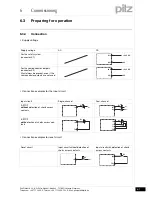
6.3.1
Function test during commissioning
Function test during commissioning
6-
Verdrahtung_multi_Basis_Betr_Funktionstest_BA
6.3.2
Commissioning the PNOZmulti safety system for the first time
Commissioning the PNOZmulti safety system for the first time
6-
Verdrahtung_multi_Basis_Betr_erstes_Mal_BA
Procedure:
`
Wire the inputs and outputs on the base unit and expansion modules
in accordance with the circuit diagram.
`
Cascading output as auxiliary output: Connect the load to CO+ and
A2, see connection example.
`
Connect the supply voltage:
– Supply voltage for the units (connector X7):
– Terminal A1: + 24 VDC
– Terminal A2: 0 V
– Supply voltage for the semiconductor outputs (connector X2):
– Terminal 24 V: + 24 VDC
– 0V terminal: 0 V
Note: Supply voltage must always be applied to X2 and X7, even if you
are not using the semiconductor outputs.
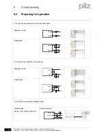
6.3.2.1
Load project from chip card
Load project from chip card
6-
Verdrahtung_multi_Basis_Betr_erstes_Mal_von_Chipkarte_BA_alt
Procedure:
`
Insert the chip card containing the current project into the card slot on
the base unit.
`
Switch on the supply voltage.
CAUTION!
It is essential to check that the safety devices operate correctly
`
after the chip card has been exchanged
`
after a project has been downloaded
`
when the project has been deleted from the base unit's mem-
ory ("Reset Project" menu)
NOTICE
Chip contacting is only guaranteed if the contact surface is
clean and undamaged. The chip's contact surface should there-
fore be protected from contamination, contact and mechanical
impact such as scratches.


