Service Modes, Error Codes, and Fault Finding
5.
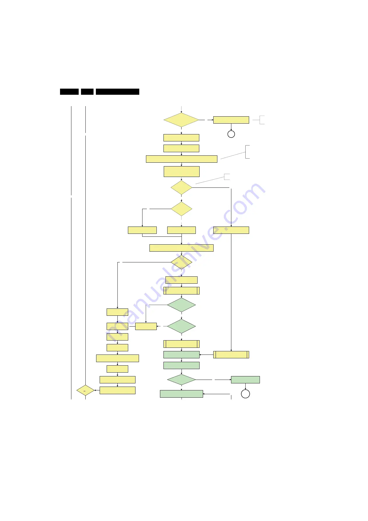
Figure 5-5 “Off” to “Semi Stand-by” flowchart (part 2)
MIPS reads the wake up reason
from standby µP.
3-th try?
No
EJTAG probe
connected ?
No
Yes
Bootscript ready
in 1250 ms?
Yes
No
Enable Alive check mechanism
Wait until AVC starts to
communicate
SW initialization
succeeded
within 20s?
No
Switch POD-MODE and ON-MODE
I/O line high.
Release AVC system reset
Feed warm boot script
Cold boot?
Yes
No
RPC start (comm. protocol)
Set I²C slave address
of Standby µP to (A0h)
Set I²C slave address
of Standby µP to (60h)
Yes
Enable the supply fault detection
algorithm
No
Yes
SP
SUPPLY-FAULT I/O line
is High?
Disable all supply related protections and
switch off the +2V5, +3V3 DC/DC converter.
switch off the remaining DC/DC
converters
Wait 5ms
Switch AVC PNX85xx
in reset (active low)
Wait 10ms
Switch the NVM reset
line HIGH.
Flash to Ram image
transfer succeeded
within 30s?
No
Yes
Code = 53
Code = 5
The supply fault line is an OR
function of DCDC, DCDC5050
and POD/CI supply switch.
An EJTAG probe (e.g. WindPower ICE probe) can
be connected for Linux Kernel debugging purposes.
Switch LOW the RESET-NVM_WP-NANDFLASH line. Add a 2ms delay before
trying to address the NVM to allow correct NVM initialization.
This will allow access to NVM and
NAND FLASH and can not be done
earlier because the FLASH needs to
be in Write Protect as long as the
supplies are not available.
Reset the Pacific by pulling LOW the Pacific
hardware reset line during 100ms.
No
Supply fault error
Detect EJTAG debug probe
(pulling pin of the probe interface to
ground by inserting EJTAG probe)
Release AVC system reset
Feed cold boot script
Release AVC system reset
Feed initializing boot script
disable alive mechanism
Boot process of the PNX5050 also starts at this point.
No
Power-ok display high ?
In case of an LCD set, check the
Power-OK display line
No
Yes
Log power-ok error and enter
protection
MP
H_17650_094
b
.ep
s
1
8
010
8


